 ChipApex | Global Electronic Components Supplier

SEARCH
Search Product
Search Post
— IC芯片 | 连接器 | 传感器 | 被动器件 —
Search productSearch post
— IC芯片 | 连接器 | 传感器 | 被动器件 —
Consult the customer manager about the wholesale price.
consultation hotline:86-132-6715-2157
email:[email protected]
Contact the product manager for consultation. One-stop consultation is available.
Do you want a lower wholesale price? Please send us your inquiry and we will reply immediately.
The NLAS4053DR2 is a triple 2:1 analog switch-multiplexer fabricated in sub-micron silicon gate CMOS technology. It operates on a single supply from 2.5 V to 5.5 V or dual supplies up to ±3 V, supporting 6 Vpp signals without coupling capacitors. The device features an SOIC-16 package and includes three independent SPDT switches with address and inhibit control pins. Key electrical parameters include a maximum on-resistance of 86 Ω at 3.0 V and 26 Ω at 4.5 V, a bandwidth of 145 MHz at 3.0 V, and propagation delays of 40 ns at 2.5 V. Address and inhibit inputs are over-voltage tolerant up to +6 V.
Verify the specific ordering suffix DR2 confirms the SOIC-16 tape and reel packaging configuration. Confirm that the component meets RoHS compliance requirements if applicable to the target assembly process. Ensure the operating temperature range of -55°C to +125°C aligns with the environmental conditions of the final application design.
Select this component when pin compatibility with legacy MC14053 or MAX4053 designs is required but improved performance metrics are needed. Consider the NLAS4053DR2 for applications demanding lower on-resistance and better linearity than standard CMOS processes provide. Verify that the 6 Vpp signal handling capability fits within the voltage constraints of the system architecture.
This part belongs to the NLAS4053 family of analog multiplexers manufactured by onsemi. It serves as an enhanced successor to older generations like the MC14053, offering superior electrical characteristics through advanced sub-micron silicon gate CMOS fabrication techniques while maintaining identical physical footprint and pinout configurations.
The datasheet explicitly identifies the NLAS4053 as a pin-for-pin replacement for the MAX4053 and MAX4053A. Designers can substitute these Maxim Integrated parts directly without modifying the PCB layout or circuit connections.
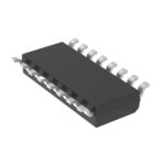 NLAS4053DR2

The activity of extra discounts on wholesale prices is in full swing…
Please fill in your contact information and we will send you the latest wholesale price list.





