 ChipApex | Global Electronic Components Supplier

SEARCH
Search Product
Search Post
— IC芯片 | 连接器 | 传感器 | 被动器件 —
Search productSearch post
— IC芯片 | 连接器 | 传感器 | 被动器件 —
Consult the customer manager about the wholesale price.
consultation hotline:86-132-6715-2157
email:[email protected]
Contact the product manager for consultation. One-stop consultation is available.
Do you want a lower wholesale price? Please send us your inquiry and we will reply immediately.
The NLAS4717MR2G is a dual independent Single Pole Double Throw (SPDT) analog switch fabricated in sub-micron silicon gate CMOS technology. It features two low on-resistance channels of 4.5 ohms at a 3.0 V supply voltage, with a guaranteed matching between switches of ±0.5 ohms. The device operates within a wide low voltage range from 1.8 V to 5.5 V and provides high bandwidth exceeding 40 MHz. Key electrical characteristics include ultra-low charge injection of ≤ 6.0 pC and low standby current of 1.0 nA maximum at 25°C. It incorporates Overvoltage Tolerance (OVT) on control pins and guarantees Break-Before-Make switching to prevent driver shorting.
Verify the ordering suffix 'MR2' corresponds to the Micro10 package format as specified in the datasheet. Confirm that the 'G' suffix indicates a lead-free compliant package. Ensure the component matches the specific pinout and marking requirements for the intended PCB layout before finalizing procurement.
Select this component when a dual SPDT analog switch with low on-resistance and high bandwidth is required. It is suitable for portable electronics operating between 1.8 V and 5.5 V. Consider the Micro10 package dimensions if space constraints are critical. Verify that the input logic levels align with the system's control voltage rails.
The NLAS4717 series includes variants such as NLAS4717FCT1G in Flip-Chip-10 packaging. The MR2G variant specifically utilizes the Micro10 package. This family is designed for portable consumer electronics requiring efficient signal routing with minimal power consumption and high signal integrity.
The datasheet notes pin-to-pin compatibility with the MAX4717. Designers should verify that the substitute part meets the same electrical specifications, particularly regarding on-resistance and bandwidth, before implementation.
The recommended operating condition specifies a DC supply voltage range of 1.8 V to 5.5 V.
Yes, the digital select input pins (Pins 4 and 8) feature Overvoltage Tolerance (OVT) to operate higher than normal supply voltages without damage.
The device guarantees an ultra-low charge injection of less than or equal to 6.0 pC.
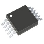 NLAS4717MR2G

The activity of extra discounts on wholesale prices is in full swing…
Please fill in your contact information and we will send you the latest wholesale price list.





