 ChipApex | Global Electronic Components Supplier

SEARCH
Search Product
Search Post
— IC芯片 | 连接器 | 传感器 | 被动器件 —
Search productSearch post
— IC芯片 | 连接器 | 传感器 | 被动器件 —
Consult the customer manager about the wholesale price.
consultation hotline:86-132-6715-2157
email:[email protected]
Contact the product manager for consultation. One-stop consultation is available.
Do you want a lower wholesale price? Please send us your inquiry and we will reply immediately.
The NLASB3157DFT2GH is a single-pole double-throw (SPDT) analog switch manufactured by onsemi. It utilizes advanced CMOS technology to provide low on-resistance and high bandwidth for signal routing. The device operates within a supply voltage range of 1.65 V to 5.5 V, ensuring compatibility with various logic families. Key electrical specifications include an on-resistance (RON) of 3 Ω and a nominal off-isolation of 57 dB at typical operating conditions. The component features two channels and is housed in a compact six-pin DFN package, suitable for space-constrained portable electronics.
Verify the exact suffix 'GH' against official onsemi documentation, as standard listings often use 'DFT2G'. Confirm the package type matches the required PCB footprint. Ensure RoHS compliance status aligns with project requirements. Cross-reference the manufacturer part number with authorized distributors to avoid counterfeit components. Validate moisture sensitivity level handling procedures during assembly.
Select this component when low on-resistance and wide bandwidth are critical for signal integrity. Consider the 1.65 V minimum supply voltage for battery-powered applications. Evaluate the DFN package size against available board space. Compare off-isolation performance if crosstalk suppression is a primary design constraint. Verify logic input compatibility with the system's control voltages.
The NLASB3157 series represents onsemi's portfolio of low-voltage analog switches designed for portable devices. This specific model belongs to the NLAS family, which emphasizes energy efficiency and small form factors. It serves as a solution for managing multiple signal sources in compact electronic designs where power consumption and physical size are limiting factors.
The NLASB3157DFT2G is a verified equivalent part number with identical functional specifications. Check for pinout compatibility before substitution. Verify that any alternative SPDT switches meet the 3 Ω on-resistance requirement. Ensure replacement packages match the existing PCB land pattern.
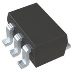 NLASB3157DFT2GH

The activity of extra discounts on wholesale prices is in full swing…
Please fill in your contact information and we will send you the latest wholesale price list.





