 ChipApex | Global Electronic Components Supplier

SEARCH
Search Product
Search Post
— IC芯片 | 连接器 | 传感器 | 被动器件 —
Search productSearch post
— IC芯片 | 连接器 | 传感器 | 被动器件 —
Consult the customer manager about the wholesale price.
consultation hotline:86-132-6715-2157
email:[email protected]
Contact the product manager for consultation. One-stop consultation is available.
Do you want a lower wholesale price? Please send us your inquiry and we will reply immediately.
The NLAST4053DR2 is a triple 2:1 analog switch-multiplexer fabricated in sub-micron Silicon Gate CMOS technology. It operates with single supplies of 3V to 5V or dual supplies up to ±3V, supporting 6Vpp signals without coupling capacitors. Key electrical parameters include a maximum on-resistance (RON) of 26Ω at VCC=3V and 5.5V, with a channel-to-channel matching (ΔRON) of 10Ω. The device features a -3dB bandwidth of 180MHz, charge injection of 12pC, and off-channel leakage current of 100nA. Switching times (Ton/Toff) are guaranteed at 23ns for VCC=4.5V. It utilizes a 16-SOIC package.
Verify component authenticity through authorized distributors as the part status is listed as obsolete. Check for RoHS compliance status, as original specifications may differ from current manufacturing runs. Confirm package integrity upon receipt, ensuring no physical damage to the SOIC-16 leads. Validate datasheet revisions against the specific lot code to ensure parameter consistency.
Select this component when low on-resistance and high linearity are required for analog signal switching. Ensure supply voltage constraints align with the 3V to 5V single or ±3V dual supply requirements. Consider the 16-SOIC package dimensions for PCB layout compatibility. Verify that the 23ns switching speed meets system timing requirements for address selection.
The NLAST4053 series represents an improved iteration of the MC14053 and MC74HC4053, designed by onsemi. It belongs to the NLAS40 family of analog switches. The DR2 suffix specifically denotes the SOIC-16 package variant supplied in tape and reel format for automated assembly processes.
Publicly confirmed pin-compatible replacements include the MAX4053 and MAX4053A. Designers should verify electrical parameter differences, particularly on-resistance and bandwidth, when substituting these alternative part numbers into existing circuits.
Yes, the device supports single supply operation between 3V and 5V by tying the VEE pin (pin 7) to ground.
The address and inhibit pins are over-voltage tolerant and can be driven up to +6V regardless of the VCC supply voltage.
When operating with a VCC of 3.0V to 3.3V, the device can interface with 1.8V logic without requiring additional translators.
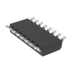 NLAST4053DR2

The activity of extra discounts on wholesale prices is in full swing…
Please fill in your contact information and we will send you the latest wholesale price list.





