 ChipApex | Global Electronic Components Supplier

SEARCH
Search Product
Search Post
— IC芯片 | 连接器 | 传感器 | 被动器件 —
Search productSearch post
— IC芯片 | 连接器 | 传感器 | 被动器件 —
Consult the customer manager about the wholesale price.
consultation hotline:86-132-6715-2157
email:[email protected]
Contact the product manager for consultation. One-stop consultation is available.
Do you want a lower wholesale price? Please send us your inquiry and we will reply immediately.
NLV14541BDR2G is listed in the Programmable Timers And Oscillators range at ChipApex. The manufacturer field lists onsemi. Its product description is IC OSC PROG TIMER 3MHZ 14SOIC. Review the specifications below when checking this part for your BOM.
The NLV14541BDR2G is an automotive-grade programmable timer IC manufactured by onsemi. It integrates a 16-stage binary counter, an internal RC oscillator, and automatic power-on reset logic. The device operates within a supply voltage range of 3.0 Vdc to 18 Vdc. Key electrical parameters include a maximum clock pulse frequency of 6.0 MHz at 15 V, propagation delays ranging from 0.9 ns to 10.5 ns depending on the output stage, and a quiescent current of up to 20 µA with auto-reset disabled. It is housed in a SOIC-14 package.
Verify that the specific order includes the 'NLV' prefix to ensure AEC-Q100 qualification and PPAP capability. Confirm the suffix 'D' indicates the SOIC-14 package and 'R2G' denotes tape and reel shipping. Check for discontinuation notices regarding related variants like the NLV14541BDG rail-pack version.
Select this component when automotive reliability standards are mandatory. Ensure the application voltage stays between 3.0 V and 18 V. For precise timing, utilize the external RC network on Pins 1 and 2, or bypass the internal oscillator by applying an external clock to Pin 3 if higher accuracy than the built-in RC is required.
This part belongs to the MC14541B family of programmable timers. The 'NLV' prefix specifically designates devices intended for automotive and other applications requiring unique site and control change requirements, distinguishing it from standard commercial grade parts.
Standard commercial equivalents include MC14541BDR2G (same package) or MC14541BDTR2G (TSSOP-14). Note that non-NLV versions lack the specific automotive qualification and PPAP documentation required for regulated automotive supply chains.
The frequency is set by an external resistor (Rtc) and capacitor (Ctc) connected to Pins 1 and 2. For frequencies between 1 kHz and 100 kHz, the formula is f ≈ 1 / (2.3 * Rtc * Ctc).
Pin 9 controls the initial output logic level after a reset. Setting it high makes the Q output initially high; setting it low makes the Q output initially low.
Yes. An external clock signal can be applied directly to Pin 3 (RS/RTC Output) to bypass the internal RC oscillator circuit.
Explore related parts through Clock/Timing, Integrated Circuits (ICs), all product categories, ChipApex homepage.
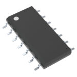 NLV14541BDR2G

The activity of extra discounts on wholesale prices is in full swing…
Please fill in your contact information and we will send you the latest wholesale price list.





