 ChipApex | Global Electronic Components Supplier

SEARCH
Search Product
Search Post
— IC芯片 | 连接器 | 传感器 | 被动器件 —
Search productSearch post
— IC芯片 | 连接器 | 传感器 | 被动器件 —
Consult the customer manager about the wholesale price.
consultation hotline:86-132-6715-2157
email:[email protected]
Contact the product manager for consultation. One-stop consultation is available.
Do you want a lower wholesale price? Please send us your inquiry and we will reply immediately.
The NLX1G11AMX1TCG is a 3-input CMOS AND gate in an ultra-small UDFN6 package. It operates at supply voltages from 1.65 V to 5.5 V with overvoltage tolerant inputs up to 7.0 V. The device features balanced propagation delays, typically 2.4 ns at 5.0 V, and provides 24 mA balanced output source and sink capability. Quiescent supply current is limited to 1.0 µA maximum at 25°C. It supports data retention down to 1.5 V and functions across temperatures from -55°C to +125°C.
Verify the specific ordering suffix to confirm the package variant, as the NLX1G11 series utilizes multiple UDFN6 dimensions including CASE 517AA, 517AQ, and 517BX. Ensure the selected part matches the required board layout and pin pitch specifications for the intended application design.
Select this component when a compact 3-input AND gate is required for low-voltage logic systems. The device is suitable for designs needing overvoltage tolerance on inputs without external protection components. Consider the available package options based on the spatial constraints of the printed circuit board assembly.
This component belongs to ON Semiconductor's advanced high-speed CMOS logic family designed for miniature surface-mount applications. The NLX1G11 series offers enhanced performance characteristics compared to standard logic gates, focusing on speed and power efficiency within a reduced physical footprint for modern electronic devices.
Check for direct substitutes within the same logic family or compatible 3-input AND gates from other manufacturers. Verify that any replacement maintains the same supply voltage range, package dimensions, and electrical characteristics to ensure functional equivalence in the existing circuit design.
The input pins are overvoltage tolerant and can withstand voltages up to 7.0 V, regardless of the applied supply voltage (VCC).
Yes, the device supports data retention at a minimum supply voltage of 1.5 V, even though recommended operating conditions start at 1.65 V.
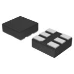 NLX1G11AMX1TCG

The activity of extra discounts on wholesale prices is in full swing…
Please fill in your contact information and we will send you the latest wholesale price list.





