 ChipApex | Global Electronic Components Supplier
SEARCH
Search Product
Search Post
— IC芯片 | 连接器 | 传感器 | 被动器件 —
Search productSearch post
— IC芯片 | 连接器 | 传感器 | 被动器件 —
Consult the customer manager about the wholesale price.
consultation hotline:86-132-6715-2157
email:[email protected]
Contact the product manager for consultation. One-stop consultation is available.
Do you want a lower wholesale price? Please send us your inquiry and we will reply immediately.
The NMUX1237 is a single-pole double-throw (SPDT) analog switch manufactured by Nexperia. It features two independent inputs/outputs (Y0, Y1) and one common input/output (Z), controlled by a digital select pin (S). The device operates on a wide supply voltage range from 1.08 V to 5.5 V with a typical ON resistance of 4 Ω at 5 V. It supports bidirectional signal paths and includes integrated overshoot suppression circuitry. The control logic maintains 1.8 V compatibility across the entire operating voltage range. The component provides Ioff protection for both digital and analog pins when unpowered.
Verify the specific ordering suffix 'GW' corresponds to the TSSOP6 plastic thin shrink small outline package (SOT363-2) with a temperature range of -40 °C to +125 °C. Confirm that the marking code 'M1' matches the physical device received. Ensure the application design accounts for the recommended operating conditions regarding switch current and voltage drops to avoid sinking GND current.
Select this component when signal integrity is critical due to its dedicated overshoot suppression feature. It is suitable for designs where power sequencing flexibility is required, as it prevents back-powering of the supply rail when unpowered. Verify that the maximum ON resistance at the lowest expected supply voltage meets the system's resistive load requirements.
The NMUX1237 belongs to the category of CMOS analog multiplexer/demultiplexer switches. It functions as a SPDT switch, distinct from higher-channel-count muxes or digital logic gates. The device utilizes standard CMOS technology optimized for low supply current and high isolation characteristics within a compact surface-mount package.
Publicly confirmed substitute part numbers are not available in the provided documentation. Designers should consult manufacturer catalogs for alternative SPDT analog switches with similar voltage ranges and logic threshold specifications.
The device implements Ioff protection on both digital and analog pins. This isolates the internal circuits when VCC is 0 V, preventing biased inputs from back-powering the supply rail and allowing flexible power sequencing without external components.
The integrated suppression circuit minimizes signal overshoot that typically occurs when switching between different channel inputs. It addresses issues related to charge injection, capacitive loads, and board parasitics to maintain signal integrity.
Yes. The digital select input (S) supports 1.8 V logic thresholds independently of the operating voltage, ensuring compatibility with low-voltage digital controllers even when the analog supply is up to 5.5 V.
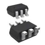 NMUX1237GWH
The activity of extra discounts on wholesale prices is in full swing…
Please fill in your contact information and we will send you the latest wholesale price list.





