ChipApex | Global Electronic Components Supplier
SEARCH
Search Product
Search Post
— IC芯片 | 连接器 | 传感器 | 被动器件 —
Search productSearch post
— IC芯片 | 连接器 | 传感器 | 被动器件 —
Consult the customer manager about the wholesale price.
consultation hotline:86-132-6715-2157
email:[email protected]
Contact the product manager for consultation. One-stop consultation is available.
Do you want a lower wholesale price? Please send us your inquiry and we will reply immediately.
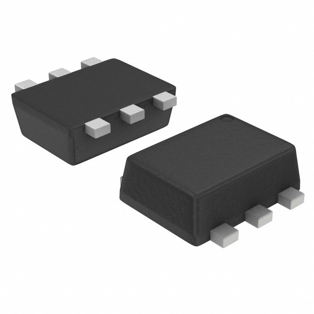
The NSVBC123JDXV6T5G is a dual NPN digital transistor from onsemi, housed in an SOT-563 surface-mount package. It integrates two NPN transistors with built-in bias resistors to simplify circuit design and reduce component count. The device supports a maximum collector-emitter voltage (VCEO) of 50 V and a continuous collector current (IC) of 100 mA. Typical input resistance values are provided for base and emitter configurations, facilitating direct interface with logic outputs. The unit operates within a temperature range of -55°C to +150°C and features a power dissipation rating of 357 mW, suitable for compact digital switching applications.
Verify the specific suffix JDXV6T5G against official onsemi documentation to confirm exact resistor ratios and tape-and-reel specifications. Ensure compatibility with standard SMT assembly processes for the SOT-563 footprint. Cross-reference the AEC-Q101 qualification status if automotive reliability requirements apply to the target application environment.
Select this component when a dual NPN configuration with integrated biasing is required for signal switching or buffering. Compare typical input resistance values against the driving source impedance to ensure adequate base current. Evaluate the thermal performance within the enclosure to maintain junction temperatures within the specified operational limits during continuous duty cycles.
This part belongs to the NSBC series of dual digital transistors manufactured by onsemi. The series offers various resistor ratio options to suit different drive conditions. The SOT-563 package provides a six-terminal solution that consolidates two complete transistor circuits into a single small outline form factor, enhancing integration density compared to discrete arrangements.
Check for pin-compatible alternatives such as the NSBC123EDXV6T1G or NSBC143TDXV6T5G, ensuring identical VCEO, IC ratings, and resistor values. Verify that any substitute maintains the same SOT-563 footprint and electrical characteristics to avoid redesigning the PCB layout or adjusting bias networks.
 NSVBC123JDXV6T5G
The activity of extra discounts on wholesale prices is in full swing…
Please fill in your contact information and we will send you the latest wholesale price list.