ChipApex | Global Electronic Components Supplier
SEARCH
Search Product
Search Post
— IC芯片 | 连接器 | 传感器 | 被动器件 —
Search productSearch post
— IC芯片 | 连接器 | 传感器 | 被动器件 —
Consult the customer manager about the wholesale price.
consultation hotline:86-132-6715-2157
email:[email protected]
Contact the product manager for consultation. One-stop consultation is available.
Do you want a lower wholesale price? Please send us your inquiry and we will reply immediately.
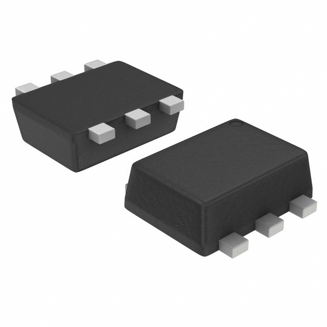
The NSVBC124EPDXV6T1G is a complementary Bias Resistor Transistor (BRT) containing one NPN and one PNP transistor with monolithic bias resistor networks. It integrates a series base resistor (R1 = 22 kΩ) and a base-emitter resistor (R2 = 22 kΩ) to replace discrete components. The device operates with a maximum collector-emitter voltage of 50 Vdc and continuous collector current of 100 mAdc. It features a DC current gain (hFE) minimum of 60 at 5.0 mA and 10 V. Thermal dissipation reaches 500 mW when both junctions are heated. The component is housed in an SOT-563 package and supports operation from -55°C to +150°C.
Verify the specific ordering suffix 'NSV' prefix indicates compliance with automotive site and control change requirements. Confirm RoHS, Pb-Free, and Halogen-Free status against the latest datasheet revision. Ensure the SOT-563 package dimensions match the target PCB layout constraints before finalizing procurement orders.
Select this component when a complementary pair of pre-biased transistors is needed for signal inversion or level shifting. The 22 kΩ input resistance values determine the drive current requirements. Verify that the 50 V breakdown voltage and 100 mA current limits exceed the application's peak operating conditions to ensure reliability under all thermal scenarios.
This part belongs to the DTC124EP series of complementary digital transistors manufactured by onsemi. It shares electrical characteristics with the NSBC124EPDXV6T1G but includes the NSV prefix denoting automotive-grade manufacturing controls. The series is designed to simplify circuit design by integrating biasing networks directly onto the silicon die within compact surface-mount packages.
NSBC124EPDXV6T1G
The device contains a monolithic bias network consisting of a series base resistor (R1) and a base-emitter resistor (R2), both typically 22 kΩ, which eliminate the need for external discrete resistors.
Yes, the NSV prefix indicates that the device is AEC-Q101 qualified and PPAP capable, meeting requirements for automotive and other applications needing unique site and control change protocols.
When both junctions are heated, the total device dissipation is 500 mW at 25°C ambient temperature, with a derating factor of 4.0 mW/°C above 25°C.
 NSVBC124EPDXV6T1G
The activity of extra discounts on wholesale prices is in full swing…
Please fill in your contact information and we will send you the latest wholesale price list.