 ChipApex | Global Electronic Components Supplier
SEARCH
Search Product
Search Post
— IC芯片 | 连接器 | 传感器 | 被动器件 —
Search productSearch post
— IC芯片 | 连接器 | 传感器 | 被动器件 —
Consult the customer manager about the wholesale price.
consultation hotline:86-132-6715-2157
email:[email protected]
Contact the product manager for consultation. One-stop consultation is available.
Do you want a lower wholesale price? Please send us your inquiry and we will reply immediately.
The NSVT65010MW6T1G is a dual matched PNP bipolar junction transistor housed in an SOT-363 package. It features a collector-emitter voltage (VCEO) of -65 V, a collector-base voltage (VCBO) of -80 V, and an emitter-base voltage (VEBO) of -5.0 V. The device supports a continuous collector current of -100 mA with a total power dissipation of 380 mW at 25 °C on an FR-5 board. Electrical characteristics include a DC current gain (hFE) ranging from 220 to 475 at -10 mA, a saturation voltage (VCE(sat)) of -650 mV max at -100 mA, and a transition frequency (fT) of 100 MHz. The operating temperature range spans from -55 °C to +150 °C.
Verify the component authenticity by checking the marking diagram against the physical package. Confirm the presence of the Pb-Free indicator and date code alignment. Ensure the ordering suffix matches the required tape and reel specifications for automated assembly processes.
Select this component when precise parameter matching is critical for circuit performance. The dual matched configuration eliminates the need for external trimming components. Verify that the -65 V rating meets the system voltage requirements and that the SOT-363 package fits the available PCB space constraints.
This part belongs to the NST65010MW6 series of dual matched general-purpose transistors. It serves as a drop-in replacement for standard discrete devices while offering superior matching characteristics. A complementary NPN equivalent, the NST65011MW6T1G, is available for designs requiring both polarities.
The complementary NPN equivalent NST65011MW6T1G is available. Direct substitution requires verifying polarity inversion and ensuring the new component's ratings align with the original design parameters.
The base-emitter voltage is matched to a difference of 2 mV or less.
Yes, the NSV prefix indicates it is AEC-Q101 qualified and PPAP capable for automotive use.
The thermal resistance (RθJA) is 328 °C/W.
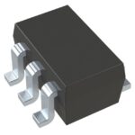 NSVT65010MW6T1G
The activity of extra discounts on wholesale prices is in full swing…
Please fill in your contact information and we will send you the latest wholesale price list.





