 ChipApex | Global Electronic Components Supplier
SEARCH
Search Product
Search Post
— IC芯片 | 连接器 | 传感器 | 被动器件 —
Search productSearch post
— IC芯片 | 连接器 | 传感器 | 被动器件 —
Consult the customer manager about the wholesale price.
consultation hotline:86-132-6715-2157
email:[email protected]
Contact the product manager for consultation. One-stop consultation is available.
Do you want a lower wholesale price? Please send us your inquiry and we will reply immediately.
The NSVTB60BDW1T1G is a dual-component semiconductor device integrating a PNP general-purpose transistor and an NPN bias resistor transistor within a single SOT-363 package. The PNP section (Q1) supports a maximum collector-emitter voltage of -50 Vdc and continuous collector current of -150 mAdc, with a DC current gain ranging from 120 to 560 at -5.0 mA. The NPN section (Q2) features a 50 Vdc collector-emitter breakdown voltage and includes monolithic bias resistors R1 and R2, providing an input resistance of approximately 22 kΩ. Total device power dissipation reaches 250 mW at 25°C ambient temperature.
Verify the specific ordering suffix against official documentation to confirm packaging orientation and tape specifications. Confirm that the NSV prefix aligns with project requirements for automotive-grade components subject to unique site controls. Ensure compliance with Pb-Free and RoHS standards as stated in the datasheet before finalizing procurement orders.
Select this component when a design requires both a standard PNP switching element and an NPN transistor with built-in biasing in a limited footprint. Evaluate the thermal resistance characteristics under actual PCB pad configurations, as total device dissipation varies significantly between minimum pad and full FR-4 pad layouts. Verify that the required current gain ranges for both transistors meet the specific application thresholds.
This part belongs to onsemi's portfolio of dual-transistor combinations designed to replace multiple discrete components. It utilizes the SOT-363 (SC-88) surface-mount technology to provide high-density integration. The device serves as a solution for mixed-signal applications where space constraints necessitate combining general-purpose bipolar junction transistors with digital bias resistor transistors.
NSVTB60BDW1T1G
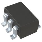 NSVTB60BDW1T1G
The activity of extra discounts on wholesale prices is in full swing…
Please fill in your contact information and we will send you the latest wholesale price list.




