 ChipApex | Global Electronic Components Supplier

SEARCH
Search Product
Search Post
— IC芯片 | 连接器 | 传感器 | 被动器件 —
Search productSearch post
— IC芯片 | 连接器 | 传感器 | 被动器件 —
Consult the customer manager about the wholesale price.
consultation hotline:86-132-6715-2157
email:[email protected]
Contact the product manager for consultation. One-stop consultation is available.
Do you want a lower wholesale price? Please send us your inquiry and we will reply immediately.
NTB0104UK-Q100Z is listed in the Translators, Level Shifters range at ChipApex. The manufacturer field lists NXP USA Inc.. Its product description is IC TRANSLATOR BIDIR 12WLCSP. Review the specifications below when checking this part for your BOM.
The NTB0104UK-Q100Z is a 4-bit dual-supply translating transceiver with auto direction sensing, enabling bidirectional voltage level translation. It features two 4-bit input-output ports (An and Bn), an output enable input (OE), and supply pins VCC(A) and VCC(B). VCC(A) operates between 1.2 V and 3.6 V, while VCC(B) ranges from 1.65 V to 5.5 V. The device supports partial power-down applications via IOFF circuitry, preventing backflow current when powered down. Qualified to AEC-Q100 Grade 1, it functions within temperature ranges of -40 °C to +85 °C and -40 °C to +125 °C.
Verify the specific package variant, WLCSP12, matches your board design constraints. Confirm that the automotive grade qualification aligns with your system requirements. Ensure supply voltage sequencing respects the operational limits where VCC(A) must not exceed VCC(B) during normal operation. Check pin compatibility for the OE and I/O connections against your schematic.
Select this component when bidirectional translation between distinct voltage domains is required without complex direction control logic. The wide supply range accommodates various low-voltage nodes. Consider the WLCSP12 package if space efficiency is critical. Verify that the input drive capability meets the minimum requirement for proper signal integrity across the translated interfaces.
This part belongs to NXP's NTB0104-Q100 family of dual-supply translating transceivers. It shares core functionality with variants like the NTB0104BQ-Q100 but differs in packaging. The UK suffix denotes the WLCSP12 wafer-level chip-size package, offering a compact footprint suitable for dense PCB layouts compared to leaded or QFN alternatives.
NTB0104BQ-Q100 offers identical electrical specifications and automotive qualification but utilizes a DHVQFN14 package instead of WLCSP12. Designers must verify mechanical fit and soldering process compatibility before substituting packages.
No special power-up sequencing is required. Either power supply can be ramped up first without damaging the device, although VCC(A) must not exceed VCC(B) during normal operation.
The OE pin should be tied to GND through a pull-down resistor to ensure the high-impedance OFF-state during power-up or power-down, preventing unintended bus activity.
Explore related parts through Logic, Integrated Circuits (ICs), all product categories, ChipApex homepage.
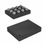 NTB0104UK-Q100Z

The activity of extra discounts on wholesale prices is in full swing…
Please fill in your contact information and we will send you the latest wholesale price list.





