 ChipApex | Global Electronic Components Supplier

SEARCH
Search Product
Search Post
— IC芯片 | 连接器 | 传感器 | 被动器件 —
Search productSearch post
— IC芯片 | 连接器 | 传感器 | 被动器件 —
Consult the customer manager about the wholesale price.
consultation hotline:86-132-6715-2157
email:[email protected]
Contact the product manager for consultation. One-stop consultation is available.
Do you want a lower wholesale price? Please send us your inquiry and we will reply immediately.
NTLJD3115PTAG is listed in the FET, MOSFET Arrays range at ChipApex. The manufacturer field lists onsemi. Its product description is MOSFET 2P-CH 20V 2.3A 6WDFN. Review the specifications below when checking this part for your BOM.
The NTLJD3115PTAG is a dual P-channel MOSFET array manufactured by onsemi. It features a drain-source voltage (V_DSS) of -20 V and a continuous drain current (I_D) of -4.6 A at 25 °C. The device utilizes a logic-level gate architecture, ensuring compatibility with standard digital logic supplies. Key electrical characteristics include a maximum gate-source threshold voltage (V_GS(th)) of -1 V at I_GS = -250 µA and a typical gate charge (Q_g) of 7.8 nC measured at V_GS = 4.5 V. The input capacitance (C_iss) is specified at 450 pF when V_DS = 10 V. The component is housed in a surface-mount 6-WDFN package with dimensions of 2x2 mm, designed for thermal efficiency with a maximum power dissipation rating of 710 mW.
Verify the specific ordering suffix against the manufacturer's official documentation to confirm exact tape-and-reel quantities and environmental compliance status. Ensure that the procurement channel sources components directly from authorized distributors to prevent counterfeit parts. Cross-reference the date code and lot number with the latest quality certificates provided by the supplier before final acceptance.
Select this component when a dual P-channel solution is required within strict spatial constraints. The -20 V rating suits low-voltage systems such as USB-powered devices or battery-operated equipment. Verify that the load current remains within the 4.6 A limit under expected operating temperatures to maintain reliability. Consider the 710 mW power dissipation limit when designing thermal paths on the PCB.
This part belongs to onsemi's Hyperjunction™ or similar advanced MOSFET portfolio, focusing on small-signal power switching applications. It complements other discrete semiconductors in the company's catalog by offering integrated dual-channel functionality. The WDFN package aligns with industry trends toward miniaturization in handheld and wearable technology sectors.
Publicly confirmed substitute part numbers are not available in the provided reference data. Engineers should consult onsemi's official replacement guide or contact technical support for validated cross-references that match the pinout, voltage ratings, and package dimensions.
Explore related parts through FETs, MOSFETs, Transistors, Discrete Semiconductor Products, all product categories.
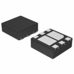 NTLJD3115PTAG

The activity of extra discounts on wholesale prices is in full swing…
Please fill in your contact information and we will send you the latest wholesale price list.





