ChipApex | Global Electronic Components Supplier

SEARCH
Search Product
Search Post
— IC芯片 | 连接器 | 传感器 | 被动器件 —
Search productSearch post
— IC芯片 | 连接器 | 传感器 | 被动器件 —
Consult the customer manager about the wholesale price.
consultation hotline:86-132-6715-2157
email:[email protected]
Contact the product manager for consultation. One-stop consultation is available.
Do you want a lower wholesale price? Please send us your inquiry and we will reply immediately.
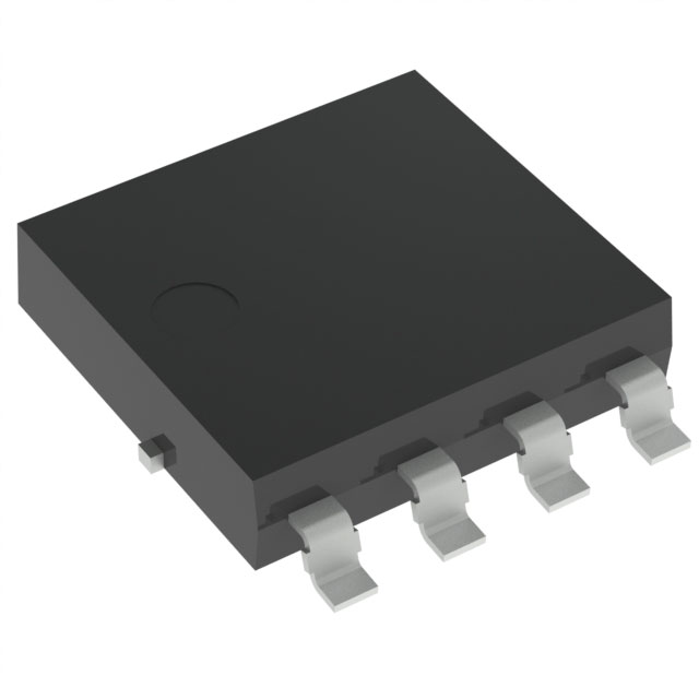
NTMJS0D9N03CGTWG is listed in the Single FETs, MOSFETs range at ChipApex. The manufacturer field lists onsemi. Its product description is MOSFET N-CH 30V LFPAK8. Review the specifications below when checking this part for your BOM.
The NTMJS0D9N03CGTWG is a single N-channel power MOSFET from onsemi, housed in an LFPAK8 (5x6mm) package. It features a drain-to-source voltage of 30 V and a maximum continuous drain current of 315 A at TC = 25°C. The device exhibits an ultra-low RDS(on) of 0.9 mΩ at VGS = 10 V and ID = 20 A. Key electrical parameters include a gate threshold voltage of 2.2 V, total gate charge of 131.4 nC, and input capacitance of 9550 pF. It supports an operating junction temperature range from -55°C to +175°C.
Verify the complete part number including the TWG suffix to ensure correct packaging specifications. Confirm that the requested quantity aligns with the standard shipping unit of 3000 units per tape and reel. Ensure compliance with RoHS and halogen-free requirements as specified in the ordering information section of the datasheet.
Select this component when high surge current handling and low conduction losses are critical. The wide SOA makes it suitable for applications requiring robust inrush current management. Evaluate thermal resistance values based on specific PCB copper pad sizes and ambient conditions rather than relying solely on steady-state ratings.
This device belongs to onsemi's portfolio of single N-channel power MOSFETs optimized for high-current switching. It utilizes the LFPAK8 case style, designated as CASE 760AA, which integrates multiple drain pins for superior heat dissipation compared to traditional packages.
Consult official cross-reference lists or contact onsemi technical support for verified substitute part numbers. Do not assume functional equivalence with other 30V MOSFETs without validating pinout compatibility and thermal performance metrics.
The maximum pulsed drain current (IDM) is rated at 900 A under steady-state conditions at TA = 25°C with a pulse width of 10 µs.
Yes, the datasheet specifies a single-pulse drain-to-source avalanche energy (EAS) rating of 556 mJ when IL(pk) equals 29.2 A.
Explore related parts through FETs, MOSFETs, Transistors, Discrete Semiconductor Products, all product categories.
 NTMJS0D9N03CGTWG

The activity of extra discounts on wholesale prices is in full swing…
Please fill in your contact information and we will send you the latest wholesale price list.