 ChipApex | Global Electronic Components Supplier

SEARCH
Search Product
Search Post
— IC芯片 | 连接器 | 传感器 | 被动器件 —
Search productSearch post
— IC芯片 | 连接器 | 传感器 | 被动器件 —
Consult the customer manager about the wholesale price.
consultation hotline:86-132-6715-2157
email:[email protected]
Contact the product manager for consultation. One-stop consultation is available.
Do you want a lower wholesale price? Please send us your inquiry and we will reply immediately.
NTS0102DP,125 is listed in the Translators, Level Shifters range at ChipApex. The manufacturer field lists NXP USA Inc.. Its product description is IC TRANSLTR BIDIRECTIONAL 8TSSOP. Review the specifications below when checking this part for your BOM.
The NTS0102DP,125 is a dual-supply translating transceiver with auto direction sensing and open-drain outputs. It features two bidirectional data ports (An, Bn) and an active HIGH output enable input (OE). Supply voltage VCC(A) operates between 1.65 V and 3.6 V, while VCC(B) operates between 2.3 V and 5.5 V. The device supports push-pull data rates up to 50 Mbit/s and includes IOFF circuitry for partial power-down applications. It is housed in an 8-lead TSSOP package and specified for ambient temperatures from -40 °C to +125 °C.
Verify the specific ordering suffix '125' corresponds to the TSSOP8 package and reel packing method. Confirm that the required temperature range of -40 °C to +125 °C matches the application environment. Ensure the design accommodates the dual supply requirements where VCC(A) must not exceed VCC(B) during normal operation.
Select this component when interfacing systems operating at different supply voltages, such as 1.8 V to 3.3 V or 3.3 V to 5.0 V. The device is suitable for point-to-point applications requiring open-drain drivers. For push-pull driver applications, verify if the NTB0102 is more appropriate based on specific performance needs.
This part belongs to the NTS0102 family of dual-supply translating transceivers. It shares functional characteristics with other packages like XSON8 but differs in physical dimensions and pin configuration. The DP variant specifically utilizes the TSSOP8 plastic thin shrink small outline package.
The NTS0102TLH is listed as a drop-in replacement for the GD package variant. Verify PCB layout compatibility regarding center pads and trace routing before substituting packages within the same product family.
The NTS0102 includes IOFF circuitry that disables all output ports when either VCC(A) or VCC(B) is switched off, preventing damaging backflow current through the device.
The Output Enable (OE) pin controls the state of the I/Os. A LOW level causes all outputs to assume a high-impedance OFF-state, while a HIGH level enables normal operation.
Explore related parts through Logic, Integrated Circuits (ICs), all product categories, ChipApex homepage.
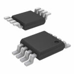 NTS0102DP,125

The activity of extra discounts on wholesale prices is in full swing…
Please fill in your contact information and we will send you the latest wholesale price list.






