 ChipApex | Global Electronic Components Supplier
SEARCH
Search Product
Search Post
— IC芯片 | 连接器 | 传感器 | 被动器件 —
Search productSearch post
— IC芯片 | 连接器 | 传感器 | 被动器件 —
Consult the customer manager about the wholesale price.
consultation hotline:86-132-6715-2157
email:[email protected]
Contact the product manager for consultation. One-stop consultation is available.
Do you want a lower wholesale price? Please send us your inquiry and we will reply immediately.
The NX3L1G66GW,125 is a low-ohmic single-pole single-throw analog switch manufactured by NXP Semiconductors. It operates within a supply voltage range of 1.4 V to 4.3 V and features an active HIGH enable input (E) with Schmitt trigger action for noise immunity. The device provides bidirectional signal transmission between terminals Y and Z with minimal attenuation due to its low ON resistance, which ranges from 0.5 Ω to 1.6 Ω depending on the supply voltage. It supports continuous current handling up to 350 mA under a 3.3 V supply and includes robust ESD protection exceeding 7500 V via HBM. The component is housed in a TSSOP5 package (SOT353-1) and is specified for operation across temperature ranges of -40 °C to +85 °C and -40 °C to +125 °C.
Verify the specific ordering suffix against the manufacturer's official documentation to confirm the exact package type and temperature rating. Ensure that the procurement channel sources components directly from authorized distributors or the manufacturer to guarantee authenticity. Cross-reference the part marking code DL with the datasheet pin configuration to validate the physical integrity of the received units before integration into designs.
Select this component when designing circuits requiring a compact analog switch with low signal loss over a wide voltage range. The TSSOP5 package is suitable for space-constrained portable applications. Consider the thermal derating characteristics above 87.5 °C when calculating power dissipation limits. Verify that the application's control signals align with the CMOS low-power consumption requirements and the specified input voltage thresholds.
The NX3L1G66 series consists of low-ohmic single-pole single-throw analog switches designed for portable electronics. The GW variant specifically utilizes a plastic thin shrink small outline package with five leads. This family of devices is engineered to handle high currents while maintaining signal integrity, making them distinct from standard digital logic switches used for data routing rather than analog signal path management.
Public confirmed substitute part numbers are not available in the provided source material.
The enable input (E) is active HIGH. When the input is LOW, the analog switch is turned off; when HIGH, it enters the ON-state allowing signal transmission.
The recommended operating conditions specify a maximum supply voltage (VCC) of 4.3 V.
Yes, the NX3L1G66 allows signals with amplitude up to VCC to be transmitted bidirectionally from terminal Y to Z or from Z to Y.
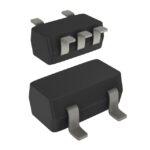 NX3L1G66GW,125
The activity of extra discounts on wholesale prices is in full swing…
Please fill in your contact information and we will send you the latest wholesale price list.





