 ChipApex | Global Electronic Components Supplier
SEARCH
Search Product
Search Post
— IC芯片 | 连接器 | 传感器 | 被动器件 —
Search productSearch post
— IC芯片 | 连接器 | 传感器 | 被动器件 —
Consult the customer manager about the wholesale price.
consultation hotline:86-132-6715-2157
email:[email protected]
Contact the product manager for consultation. One-stop consultation is available.
Do you want a lower wholesale price? Please send us your inquiry and we will reply immediately.
The NX3L1T53GT,115 is a low-ohmic single-pole double-throw analog switch manufactured by NXP USA Inc. It operates on a single supply voltage ranging from 1.4 V to 4.3 V and features an active LOW enable input (E), a digital select input (S), and two independent inputs/outputs (Y0, Y1) with a common port (Z). The device provides a peak ON resistance of up to 4.1 Ω at 1.4 V and 0.9 Ω at higher voltages. It supports continuous switch currents of 350 mA and includes Schmitt trigger action for noise immunity. The component is housed in an XSON8 package (SOT833-1) with dimensions of 1 x 1.95 x 0.5 mm and is rated for operation between -40 °C and +125 °C.
Verify the specific ordering suffix against the manufacturer's current documentation to confirm the exact package variant and temperature range. Confirm RoHS compliance status and REACH registration details directly with the supplier or official datasheet before finalizing procurement specifications.
Select this component when a single SPDT switch with low ON resistance is required within a 1.4 V to 4.3 V supply range. Ensure the application requires the XSON8 package format and can accommodate the specified thermal derating characteristics above 118 °C.
This part belongs to the NX3L1T53 series of low-ohmic analog switches. Other variants in the family include the NX3L1T53GD and NX3L1T53GM, which utilize different package footprints such as SOT996-2 and SOT902-2 while maintaining identical electrical performance and functionality.
Publicly confirmed substitute part numbers are not available in the provided source material. Verify compatibility with existing circuit designs if considering alternative manufacturers.
The device features low threshold digital inputs that allow it to be driven by 1.8 V logic levels even in 3.3 V applications without significantly increasing supply current.
The total power dissipation is 250 mW at ambient temperatures between -40 °C and +125 °C, with linear derating starting above 118 °C.
Yes, signals can be transmitted from Z to Y0/Y1 or from Y0/Y1 to Z, allowing for flexible multiplexer/demultiplexer configurations.
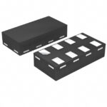 NX3L1T53GT,115
The activity of extra discounts on wholesale prices is in full swing…
Please fill in your contact information and we will send you the latest wholesale price list.





