 ChipApex | Global Electronic Components Supplier
SEARCH
Search Product
Search Post
— IC芯片 | 连接器 | 传感器 | 被动器件 —
Search productSearch post
— IC芯片 | 连接器 | 传感器 | 被动器件 —
Consult the customer manager about the wholesale price.
consultation hotline:86-132-6715-2157
email:[email protected]
Contact the product manager for consultation. One-stop consultation is available.
Do you want a lower wholesale price? Please send us your inquiry and we will reply immediately.
The NX3L2267SGU,115 is a dual low-ohmic single-pole double-throw analog switch manufactured by NXP USA Inc. It operates within a supply voltage range of 1.4 V to 4.3 V and supports an ambient temperature range from -40 °C to +125 °C. The device features a typical ON resistance of 0.5 Ω at 2.7 V and 4.3 V, with a maximum OFF-state leakage current of 200 nA at 4.3 V. It provides a -3 dB frequency response of 60 MHz and isolation of -90 dB at 100 kHz. The component utilizes a 10-terminal XQFN package (SOT1160-1) with dimensions of 1.40 x 1.80 x 0.50 mm.
Verify the specific ordering suffix '115' against official NXP documentation to confirm tape-and-reel packaging specifications. Ensure the selected variant matches the required SOT1160-1 package dimensions and thermal characteristics for the target application environment.
Select this component when designing circuits requiring low signal attenuation and minimal distortion. The device is suitable for applications needing high noise immunity and compatibility with 1.8 V control logic while handling signals up to 4.3 V. Consider the 1.40 x 1.80 mm footprint for space-constrained portable designs.
The NX3L2267 series includes variants such as NX3L2267GM and NX3L2267GU. The NX3L2267SGU,115 specifically corresponds to the SOT1160-1 package type. This family serves as a low-ohmic dual SPDT analog switch designed for multiplexing and demultiplexing applications in consumer electronics.
NX3L2267GM,115
Yes, the device allows signals with amplitude up to VCC to be transmitted between the common port (nZ) and independent ports (nY0 or nY1).
Latch-up performance exceeds 100 mA per JESD 78B Class II Level A.
The control input accepts voltages above the supply voltage, allowing flexibility in logic level interfacing.
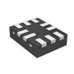 NX3L2267SGU,115
The activity of extra discounts on wholesale prices is in full swing…
Please fill in your contact information and we will send you the latest wholesale price list.





