 ChipApex | Global Electronic Components Supplier
SEARCH
Search Product
Search Post
— IC芯片 | 连接器 | 传感器 | 被动器件 —
Search productSearch post
— IC芯片 | 连接器 | 传感器 | 被动器件 —
Consult the customer manager about the wholesale price.
consultation hotline:86-132-6715-2157
email:[email protected]
Contact the product manager for consultation. One-stop consultation is available.
Do you want a lower wholesale price? Please send us your inquiry and we will reply immediately.
The NX3L4051HR,118 is a single low-ohmic 8-channel analog switch manufactured by NXP Semiconductors. It operates on a single supply voltage ranging from 1.4 V to 4.3 V and features three digital select inputs (S1 to S3) and one enable input (E). The device includes eight independent bidirectional inputs/outputs (Y0 to Y7) and a common input/output (Z). It provides very low ON resistance, typically 0.5 Ω at 4.3 V, with a maximum of 0.9 Ω across the full temperature range. The component supports break-before-make switching and high noise immunity.
Verify the specific ordering suffix against the manufacturer's documentation to ensure correct packaging and tape specifications. Confirm that the package type matches the required thermal and footprint constraints for the target PCB design. Cross-reference the revision history to ensure compatibility with existing system designs.
Select this component when an 8-channel analog switch is required within a 1.4 V to 4.3 V supply range. Ensure the application benefits from the low ON resistance and flatness characteristics for minimal signal attenuation. Verify that the HXQFN16 package dimensions fit the available board space and thermal requirements.
This part belongs to the NX3L4051 series of low-ohmic analog switches. It shares functional similarities with other members like the NX3L4051PW but differs in package configuration. The HR variant utilizes the HXQFN16 package, while the PW variant uses TSSOP16. Both share identical electrical characteristics and pinout functionality.
NX3L4051PW serves as a direct package alternative offering identical electrical performance in a TSSOP16 form factor. Designers requiring a different footprint should verify pin-to-pin compatibility and thermal dissipation capabilities before substitution.
Yes, the low threshold digital inputs allow the device to be driven by 1.8 V logic levels in 3.3 V applications without a significant increase in supply current, enabling it to switch 4.3 V signals.
At VCC = 3.6 V to 4.3 V, the maximum OFF-state leakage current is ±50 nA at 25 °C and ±500 nA at +125 °C.
Yes, break-before-make switching is guaranteed by design to prevent short circuits during channel transitions.
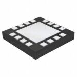 NX3L4051HR,115
The activity of extra discounts on wholesale prices is in full swing…
Please fill in your contact information and we will send you the latest wholesale price list.





