 ChipApex | Global Electronic Components Supplier
SEARCH
Search Product
Search Post
— IC芯片 | 连接器 | 传感器 | 被动器件 —
Search productSearch post
— IC芯片 | 连接器 | 传感器 | 被动器件 —
Consult the customer manager about the wholesale price.
consultation hotline:86-132-6715-2157
email:[email protected]
Contact the product manager for consultation. One-stop consultation is available.
Do you want a lower wholesale price? Please send us your inquiry and we will reply immediately.
The NX3V1G66GW,125 is a low-ohmic single-pole single-throw analog switch manufactured by NXP Semiconductors. It operates within a supply voltage range of 1.4 V to 4.3 V and features an active HIGH enable input (E). The device utilizes Schmitt trigger action at the enable pin for tolerance to slow input transitions. Key electrical parameters include an ultra-low ON resistance ranging from 0.25 Ω to 0.8 Ω depending on VCC, and high noise immunity with ESD protection exceeding 7500 V (HBM) and 6000 V (IEC61000-4-2 contact discharge). It supports bidirectional signal transmission up to VCC amplitude.
Verify the specific ordering suffix ',125' against official NXP documentation to confirm tape-and-reel packaging details, as datasheet tables list 'NX3V1G66GW' under SOT353 without explicit reel specifications in the provided text. Ensure the component meets the required temperature range of -40 °C to +125 °C for the intended application environment.
Select this component when a single-channel analog switch with very low ON resistance is required for portable applications. Consider the TSSOP5 package dimensions if board space allows, noting the thermal derating characteristics above 87.5 °C. Verify that the operating voltage aligns with the 1.4 V to 4.3 V range and that the enable logic polarity matches the system design.
The NX3V1G66 series includes variants such as NX3V1G66GM in an XSON6 package. The GW variant specifically denotes the TSSOP5 plastic thin shrink small outline package (SOT353-1). This part belongs to NXP's low-voltage analog switch portfolio designed for consumer electronics requiring high current handling and low power consumption.
Publicly confirmed substitute part numbers are not available in the provided source material. Designers should consult NXP directly or verify cross-reference data through official distributor channels before replacing this component.
The enable input (E) is active HIGH. When pin E is LOW, the analog switch is turned off; when HIGH, it is in the ON-state.
Schmitt trigger action at the enable input (E) makes the circuit tolerant to slower input rise and fall times.
The device has a high current handling capability of 500 mA continuous current under a 3.3 V supply.
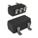 NX3V1G66GW,125
The activity of extra discounts on wholesale prices is in full swing…
Please fill in your contact information and we will send you the latest wholesale price list.





