 ChipApex | Global Electronic Components Supplier

SEARCH
Search Product
Search Post
— IC芯片 | 连接器 | 传感器 | 被动器件 —
Search productSearch post
— IC芯片 | 连接器 | 传感器 | 被动器件 —
Consult the customer manager about the wholesale price.
consultation hotline:86-132-6715-2157
email:[email protected]
Contact the product manager for consultation. One-stop consultation is available.
Do you want a lower wholesale price? Please send us your inquiry and we will reply immediately.
NX5DV330PW,112 is listed in the Analog Switches - Special Purpose range at ChipApex. The manufacturer field lists NXP USA Inc.. Its product description is IC VIDEO MUX/DEMUX 1X2 16TSSOP. Review the specifications below when checking this part for your BOM.
The NX5DV330PW,112 is a quad 1-of-2 high-speed TTL-compatible video multiplexer/demultiplexer manufactured by NXP Semiconductors. It operates within a supply voltage range of 4.0 V to 5.5 V and supports an ambient temperature range from −40 °C to +85 °C. The device features four independent switches with a maximum on-resistance of 10 Ω at 5 V. Key dynamic characteristics include a typical turn-on time of 4.0 ns and a maximum propagation delay of 6.0 ns. The component utilizes a TSSOP16 plastic thin shrink small outline package (SOT403-1) with a body width of 4.4 mm.
Verify the specific ordering suffix '112' corresponds to the TSSOP16 package variant when sourcing. Confirm the manufacturer is NXP Semiconductors to ensure authenticity. Check current product status as older revisions may be discontinued. Ensure environmental compliance requirements match the datasheet specifications before procurement.
Select this component for designs requiring a quad 1-of-2 video switch with TTL-compatible logic levels. The TSSOP16 package is suitable for surface-mount assembly where space efficiency is required. Verify that the operating voltage remains between 4.0 V and 5.5 V. Consider the 10 Ω maximum on-resistance for signal integrity requirements in the target application circuit.
This part belongs to the NX5DV330 family of video multiplexer/demultiplexers. Other variants in the series include the SO16 (NX5DV330D), SSOP16 (NX5DV330DS), and DHVQFN16 (NX5DV330BQ) packages. All variants share identical electrical characteristics and functional descriptions, differing only in physical packaging dimensions and lead configurations.
Direct pin-to-pin replacements within the same family include NX5DV330D, NX5DV330DS, and NX5DV330BQ. These alternatives offer identical electrical performance but utilize different package types such as SO16, SSOP16, or DHVQFN16. Ensure the PCB footprint matches the selected package variant before substitution.
The enable input (E) is active LOW. When E is HIGH, all switches are turned off. When E is LOW, the switches operate based on the state of the select input (S).
Schmitt-trigger action at the enable input (E) and select input (S) makes the circuit tolerant to slower input rise and fall times across the entire VCC range from 4.0 V to 5.5 V.
The total power dissipation (Ptot) is rated at 500 mW. For the TSSOP16 package, power derates linearly with 5.5 mW/K above 60 °C.
Explore related parts through Interface, Integrated Circuits (ICs), all product categories, ChipApex homepage.
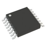 NX5DV330PW,112

The activity of extra discounts on wholesale prices is in full swing…
Please fill in your contact information and we will send you the latest wholesale price list.





