 ChipApex | Global Electronic Components Supplier

SEARCH
Search Product
Search Post
— IC芯片 | 连接器 | 传感器 | 被动器件 —
Search productSearch post
— IC芯片 | 连接器 | 传感器 | 被动器件 —
Consult the customer manager about the wholesale price.
consultation hotline:86-132-6715-2157
email:[email protected]
Contact the product manager for consultation. One-stop consultation is available.
Do you want a lower wholesale price? Please send us your inquiry and we will reply immediately.
NXS0104GU12X is listed in the Specialty Logic range at ChipApex. The manufacturer field lists Nexperia USA Inc.. Its product description is NXS0104GU12/SOT1174/XQFN12. Review the specifications below when checking this part for your BOM.
The NXS0104GU12X is a 4-bit dual supply translating transceiver with auto direction sensing, housed in an XQFN12 package (SOT1174-1). It supports bidirectional voltage level translation between VCC(A) ranging from 1.65 V to 3.6 V and VCC(B) ranging from 2.3 V to 5.5 V. The device features open-drain outputs, IOFF circuitry for partial power-down applications, and ESD protection exceeding 8000 V contact discharge on the B port. It operates within an ambient temperature range of -40 °C to +125 °C.
Verify that the ordering suffix 'X' corresponds to the specific reel or cut tape packaging configuration required for your assembly line. Confirm the SOT1174-1 XQFN12 package dimensions match your PCB footprint design. Ensure the selected variant meets the -40 °C to +125 °C operating temperature requirements for your target environment.
Select this component when interfacing systems with distinct supply voltages where VCC(A) must not exceed VCC(B). The open-drain output type is optimal for bus architectures like I2C. Consider the XQFN12 package size constraints against available board space. Verify that the external driver impedance remains below 50 Ω to maintain specified data rates and transition times.
The NXS0104GU12X belongs to the NXS0104 family of dual supply translating transceivers manufactured by Nexperia. This family includes variants with different package options such as TSSOP14, DHVQFN14, and WLCSP12. All variants share identical electrical characteristics and functional descriptions, differing only in physical form factor and pinout arrangement.
NXS0104PWJ
The NXS0104GU12X includes IOFF circuitry that disables all output ports when either VCC(A) or VCC(B) is at ground potential, preventing damaging backflow current through the device.
No special power-up sequencing is required. While VCC(A) must be less than or equal to VCC(B) during operation, the device can withstand VCC(A) being higher than VCC(B) during the power-up ramp phase without damage.
Explore related parts through Logic, Integrated Circuits (ICs), all product categories, ChipApex homepage.
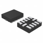 NXS0104GU12X

The activity of extra discounts on wholesale prices is in full swing…
Please fill in your contact information and we will send you the latest wholesale price list.





