 ChipApex | Global Electronic Components Supplier

SEARCH
Search Product
Search Post
— IC芯片 | 连接器 | 传感器 | 被动器件 —
Search productSearch post
— IC芯片 | 连接器 | 传感器 | 被动器件 —
Consult the customer manager about the wholesale price.
consultation hotline:86-132-6715-2157
email:[email protected]
Contact the product manager for consultation. One-stop consultation is available.
Do you want a lower wholesale price? Please send us your inquiry and we will reply immediately.
NXS0104PW-Q100J is listed in the Specialty Logic range at ChipApex. The manufacturer field lists Nexperia USA Inc.. Its product description is NXS0104PW-Q100/SOT402/TSSOP14. Review the specifications below when checking this part for your BOM.
The NXS0104PW-Q100J is a 4-bit dual supply translating transceiver with auto direction sensing, housed in a TSSOP14 (SOT402-1) package. It supports bidirectional voltage level translation between VCCA (1.65 V to 3.6 V) and VCCB (2.3 V to 5.5 V). The device features open-drain outputs, an active HIGH output enable input (OE), and IOFF circuitry for partial power-down mode operation. Qualified to AEC-Q100 Grade 1 standards, it operates within an ambient temperature range of -40 °C to +125 °C.
Verify the specific ordering suffix 'J' against the manufacturer's official documentation to confirm exact packaging and marking details. Ensure the selected component matches the required temperature grade and package variant specified in the design. Cross-reference the datasheet revision date to validate all electrical characteristics and application notes prior to final procurement.
Select this component when interfacing systems requiring bidirectional translation between low-voltage logic (1.65 V–3.6 V) and higher-voltage nodes (up to 5.5 V). The auto-direction feature simplifies design by eliminating manual direction control. Verify that the open-drain output type aligns with the target bus requirements, as push-pull alternatives may be needed for other driver types.
This part belongs to the Nexperia NXS0104-Q100 family of dual supply translating transceivers. It is specifically designed for automotive electronics, meeting rigorous reliability standards. The PW suffix indicates the TSSOP14 plastic thin shrink small outline package, providing a compact solution for space-constrained PCB layouts while maintaining robust electrical performance across wide temperature ranges.
NXS0104GU12-Q100X
During power-up, VCCA can be greater than or equal to VCCB without damaging the device. Special sequencing is not required, but the IOFF circuitry disables outputs if either supply is at ground potential.
The Output Enable (OE) pin controls the state of the I/O ports. Setting OE to LOW places all outputs in a high-impedance OFF-state, while HIGH enables normal translation operation.
Explore related parts through Logic, Integrated Circuits (ICs), all product categories, ChipApex homepage.
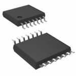 NXS0104PW-Q100J

The activity of extra discounts on wholesale prices is in full swing…
Please fill in your contact information and we will send you the latest wholesale price list.






