 ChipApex | Global Electronic Components Supplier

SEARCH
Search Product
Search Post
— IC芯片 | 连接器 | 传感器 | 被动器件 —
Search productSearch post
— IC芯片 | 连接器 | 传感器 | 被动器件 —
Consult the customer manager about the wholesale price.
consultation hotline:86-132-6715-2157
email:[email protected]
Contact the product manager for consultation. One-stop consultation is available.
Do you want a lower wholesale price? Please send us your inquiry and we will reply immediately.
NXS0506UPZ is listed in the Translators, Level Shifters range at ChipApex. The manufacturer field lists Nexperia USA Inc.. Its product description is IC TRANSLATOR BIDIR 16WLCSP. Review the specifications below when checking this part for your BOM.
The NXS0506UP is an SD 3.0-compatible bidirectional dual supply level translator with auto-direction control, EMI filter, and ESD protection. It interfaces memory cards (1.7 V to 3.6 V) with hosts (1.1 V to 1.95 V). Supported modes include SDR104 (208 MHz), SDR50, DDR50, SDR25, SDR12, High-Speed (50 MHz), and Default-Speed (25 MHz). The device operates from -40 °C to +85 °C. It features integrated pull-up resistors (typical 70 kΩ) and series resistors (22.5 Ω host, 15 Ω card side). Supply currents are typically 4 µA (host) and 7 µA (card). Propagation delays range from 1.6 ns to 5.8 ns depending on voltage levels.
Verify the specific package suffix matches the design requirement: UP denotes WLCSP16 (SOT8025-1) while GU denotes XQFN16 (SOT1161-1). Confirm that the host supply voltage remains within the 1.1 V to 1.95 V range and the card supply stays between 1.7 V and 3.6 V. Ensure PCB layout guidelines for the chosen package type are followed to maintain signal integrity at high clock rates.
Select this component when interfacing low-voltage hosts (1.1 V–1.95 V) with standard or high-speed SD cards requiring voltage translation up to 3.6 V. It is suitable for designs needing integrated EMI suppression and robust ESD protection without external discrete components. Consider the WLCSP16 package for minimal footprint or XQFN16 for alternative mounting needs. Verify compatibility with SD 3.0 signaling modes if operating above 50 MHz.
The NXS0506UP is the WLCSP16 variant of the NXS0506 family, which also includes the NXS0506GU in an XQFN16 package. Both variants share identical electrical characteristics and functionality but differ in physical package dimensions and pinout mapping. The UP package utilizes a 16-bump wafer-level chip-scale format with a 0.35 mm pitch, designed for space-constrained mobile applications.
Public confirmed substitute part numbers are not provided in the source material.
Yes, the internal design of channels DAT0, DAT1, DAT2, DAT3, and CMD is identical. They can be exchanged to ease PCB layout issues without impacting functionality.
The device has an auto-enable feature; it enables when VCCB rises above 1.5 V and disables when VCCB drops below 0.65 V.
The CLKFB pin provides a feedback clock path from the host to compensate for delay introduced by the translator and PCB tracks, improving timing margin for data read-back from the memory card.
Explore related parts through Logic, Integrated Circuits (ICs), all product categories, ChipApex homepage.
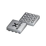 NXS0506UPZ

The activity of extra discounts on wholesale prices is in full swing…
Please fill in your contact information and we will send you the latest wholesale price list.






