 ChipApex | Global Electronic Components Supplier

SEARCH
Search Product
Search Post
— IC芯片 | 连接器 | 传感器 | 被动器件 —
Search productSearch post
— IC芯片 | 连接器 | 传感器 | 被动器件 —
Consult the customer manager about the wholesale price.
consultation hotline:86-132-6715-2157
email:[email protected]
Contact the product manager for consultation. One-stop consultation is available.
Do you want a lower wholesale price? Please send us your inquiry and we will reply immediately.
NXU0101GW-Q100H is listed in the Translators, Level Shifters range at ChipApex. The manufacturer field lists Nexperia USA Inc.. Its product description is NXU0101GW-Q100/SOT363/SC-88. Review the specifications below when checking this part for your BOM.
The NXU0101GW-Q100H is a 1-bit dual-supply level translating buffer with Schmitt-trigger input and 3-state output. It facilitates asynchronous communication between data buses, supporting unidirectional translation from the A bus to the B bus. Both VCCA and VCCB operate within a range of 0.9 V to 5.5 V. The device features an output enable (OE) pin for high-impedance isolation and IOFF circuitry for partial power-down protection. It supports maximum data rates up to 250 Mbps and operates across temperatures from -40 °C to +125 °C.
Verify the specific suffix 'GW' corresponds to the SOT363-2 package type required for your PCB layout. Confirm that the automotive qualification grade aligns with your system's reliability standards. Ensure the OE pin configuration matches your power sequencing requirements to maintain the high-impedance state correctly.
Select this component when bidirectional translation is not required but unidirectional buffering with level shifting is needed. The Schmitt trigger makes it suitable for noisy environments. Consider the 3-state output if bus isolation is necessary. Verify that the supply voltage ranges on both sides fall within the 0.9 V to 5.5 V specification.
This part belongs to Nexperia's automotive-grade logic portfolio, qualified under AEC-Q100 Grade 1. It complements other level translators like the LSF0101 and NXS0101 series by offering a dedicated unidirectional buffer with 3-state control rather than bidirectional translation capabilities.
NXU0101GM-Q100H (XSON6 package)
If either VCCA or VCCB is disconnected or drops below 100 mV, the device enters suspend mode, placing the output in a high-impedance state.
The Output Enable (OE) pin controls the 3-state output. When set LOW, the output is disabled and isolated; when HIGH, the buffer is active.
Explore related parts through Logic, Integrated Circuits (ICs), all product categories, ChipApex homepage.
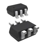 NXU0101GW-Q100H

The activity of extra discounts on wholesale prices is in full swing…
Please fill in your contact information and we will send you the latest wholesale price list.







