 ChipApex | Global Electronic Components Supplier

SEARCH
Search Product
Search Post
— IC芯片 | 连接器 | 传感器 | 被动器件 —
Search productSearch post
— IC芯片 | 连接器 | 传感器 | 被动器件 —
Consult the customer manager about the wholesale price.
consultation hotline:86-132-6715-2157
email:[email protected]
Contact the product manager for consultation. One-stop consultation is available.
Do you want a lower wholesale price? Please send us your inquiry and we will reply immediately.
OR2T15B8S208-DB is listed in the Field Programmable Gate Array range at ChipApex. The manufacturer field lists Lattice Semiconductor Corporation. Its product description is FPGA, 400 CLBS, 19200 GATES. Review the specifications below when checking this part for your BOM.
The OR2T15B8S208-DB is a Field Programmable Gate Array (FPGA) from the Lattice OR2TxxA/B family, manufactured using 0.3 µm CMOS technology. It features 784 logic cells and supports up to 480 user I/Os, which are 5 V tolerant for mixed-voltage interfacing. The device utilizes four 16-bit look-up tables per programmable function unit (PFU) to implement bus structures. Key electrical parameters include a maximum operating frequency (fMAX) of 360 MHz, propagation delay (tPD) of 3.0 ns, clock-to-output delay (tCO) of 2.9 ns, and setup time (tS) of 2.0 ns. It operates within a temperature range of -40 °C to 85 °C and requires 3.3 V or 3.3/5 V power supplies.
Verify the specific suffix 'DB' against official Lattice documentation to confirm package type and temperature grade. Ensure compatibility with 3.3 V or 3.3/5 V supply rails as specified in the datasheet. Confirm RoHS status if required by your manufacturing standards, as some older OR2T variants may not be compliant. Cross-reference the PBGA256 footprint dimensions during PCB layout.
Select this component when 784 logic cells and high I/O density are required for 5 V tolerant applications. Compare against the OR2CxxA series if lower cost is prioritized over speed, noting the 0.35 µm process difference. Consider the OR2TxxB variant if higher performance grades are needed beyond the standard specifications provided for this model.
This part belongs to the Lattice OR2TxxA/B FPGA family, designed for high-performance interfacing and switching. It represents an evolution from the OR2CxxA series, utilizing a faster 0.3 µm CMOS process. The family is characterized by its ability to handle large bus structures and provide flexible I/O configurations for complex system integration tasks.
Direct replacements within the same family include other OR2TxxB variants with different cell counts or speed grades. Verify pinout compatibility before substituting with OR2TxxA models, as process node differences may affect timing characteristics.
Explore related parts through Embedded, Integrated Circuits (ICs), all product categories, ChipApex homepage.


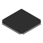 OR2T15B8S208-DB

The activity of extra discounts on wholesale prices is in full swing…
Please fill in your contact information and we will send you the latest wholesale price list.



