 ChipApex | Global Electronic Components Supplier
SEARCH
Search Product
Search Post
— IC芯片 | 连接器 | 传感器 | 被动器件 —
Search productSearch post
— IC芯片 | 连接器 | 传感器 | 被动器件 —
Consult the customer manager about the wholesale price.
consultation hotline:86-132-6715-2157
email:[email protected]
Contact the product manager for consultation. One-stop consultation is available.
Do you want a lower wholesale price? Please send us your inquiry and we will reply immediately.
The PBLS1501V is a low VCEsat PNP transistor and NPN resistor-equipped transistor integrated into a single SOT666 plastic surface-mounted package. It functions as a 15 V loadswitch with a maximum collector-emitter voltage of -15 V for the PNP section and 50 V for the NPN section. The device supports a DC collector current of -500 mA for the PNP transistor and 100 mA for the NPN output. Key electrical parameters include an equivalent on-resistance (RCEsat) of up to 500 mΩ at -500 mA, a bias resistor (R1) ranging from 1.54 kΩ to 2.86 kΩ, and a total power dissipation limit of 300 mW per device.
Verify the specific ordering suffix against the manufacturer's official documentation to ensure correct packing quantity and tape-and-reel specifications. Confirm the marking code 'C1' matches the intended production batch. Check the most recent product status data sheet to confirm availability and any potential changes to legal definitions or disclaimers before finalizing procurement orders.
Select the PBLS1501V when a combined PNP loadswitch and NPN driver is required in a small footprint. Ensure the application voltage does not exceed the -15 V collector-emitter rating for the PNP section. Verify that the thermal resistance of 416 K/W in free air is acceptable for the expected ambient temperature and power dissipation levels in the target design environment.
This component belongs to Nexperia's portfolio of low VCEsat transistors designed for efficient switching applications. It serves as an alternative to discrete component arrangements, offering reduced PCB area and pick-and-place costs. The SOT666 package variant provides a compact surface-mount option compared to the standard SC-88 package used in the PBLS1501Y counterpart.
The PBLS1501Y is the primary functional substitute, sharing identical electrical characteristics but utilizing the SOT363 (SC-88) package instead of the SOT666. Designers must verify pinout compatibility and physical footprint differences when substituting between these two package types.
The NPN section acts as a resistor-equipped transistor (RET) with an integrated bias resistor (R1), providing a low-threshold switch interface that requires less drive power than comparable MOSFETs.
The total power dissipation per device is limited to 300 mW, with a junction temperature maximum of 150 °C and an ambient temperature range of -65 °C to +150 °C.
The primary difference is the package type; the PBLS1501V uses the SOT666 package, while the PBLS1501Y uses the SOT363 (SC-88) package. Both share the same internal circuitry and electrical specifications.
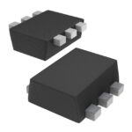 PBLS1501V,115
The activity of extra discounts on wholesale prices is in full swing…
Please fill in your contact information and we will send you the latest wholesale price list.




