ChipApex | Global Electronic Components Supplier
SEARCH
Search Product
Search Post
— IC芯片 | 连接器 | 传感器 | 被动器件 —
Search productSearch post
— IC芯片 | 连接器 | 传感器 | 被动器件 —
Consult the customer manager about the wholesale price.
consultation hotline:86-132-6715-2157
email:[email protected]
Contact the product manager for consultation. One-stop consultation is available.
Do you want a lower wholesale price? Please send us your inquiry and we will reply immediately.
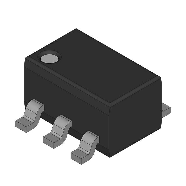
The PBLS1501Y,115 is a dual-transistor load switch in an SOT363 (SC-88) package. It integrates a low VCEsat PNP transistor (TR1) and an NPN resistor-equipped transistor (TR2). TR1 supports a collector-emitter voltage of -15 V and DC current up to -500 mA with typical on-resistance of 300 mΩ. TR2 provides a collector-emitter voltage of 50 V and output current up to 100 mA, featuring a bias resistor R1 of 2.2 kΩ. The device operates within an ambient temperature range of -55 °C to +150 °C.
Verify the specific ordering suffix matches the required packing method. The PBLS1501Y variant utilizes the SOT363 package. Confirm the marking code corresponds to the manufacturing origin. Ensure the data sheet revision aligns with current design requirements before finalizing procurement specifications.
Select this component when a combined high-side PNP switch and controlled NPN load switch are needed in minimal PCB area. The integrated bias resistor simplifies the drive circuit for the NPN section. Verify that the -15 V rating for the PNP section meets the supply line requirements and that the 50 V rating for the NPN section is sufficient for the intended load voltage.
This part belongs to the PBLS1501 series, which includes the PBLS1501V variant housed in an SOT666 package. Both variants share identical electrical characteristics but differ in physical footprint. The PBLS1501Y specifically denotes the SC-88 plastic surface-mounted package configuration.
The PBLS1501V serves as a pin-compatible alternative with a different package outline (SOT666). No other direct substitutes are documented in the provided datasheet.
The internal resistor (R1) is connected to the base of the NPN transistor (TR2), eliminating the need for an external bias resistor and reducing the overall component count.
The device features a low threshold voltage of less than 1 V, requiring lower drive power compared to standard MOSFETs.
The maximum DC collector current for the PNP transistor (TR1) is -500 mA.
 PBLS1501Y,115
The activity of extra discounts on wholesale prices is in full swing…
Please fill in your contact information and we will send you the latest wholesale price list.