 ChipApex | Global Electronic Components Supplier
SEARCH
Search Product
Search Post
— IC芯片 | 连接器 | 传感器 | 被动器件 —
Search productSearch post
— IC芯片 | 连接器 | 传感器 | 被动器件 —
Consult the customer manager about the wholesale price.
consultation hotline:86-132-6715-2157
email:[email protected]
Contact the product manager for consultation. One-stop consultation is available.
Do you want a lower wholesale price? Please send us your inquiry and we will reply immediately.
The PBLS1502Y is a 15 V PNP BISS loadswitch integrating a low VCEsat PNP transistor and an NPN resistor-equipped transistor in a single SOT363 package. The PNP section (TR1) supports a collector current of -500 mA with a maximum on-resistance of 500 mΩ at -500 mA. The NPN section (TR2) features a 50 V collector-emitter voltage rating, 100 mA output current, and a typical bias resistor of 4.7 kΩ. Total power dissipation is limited to 300 mW per device.
Verify the specific ordering suffix against the manufacturer's current database to confirm availability status. The datasheet indicates this product may be subject to change or end-of-life notices. Confirm the package type matches the required PCB footprint before procurement. Ensure compliance with the absolute maximum ratings during design validation.
Select this component when space constraints require combining switching and control functions. The integrated NPN transistor simplifies drive circuits by eliminating external base resistors. Verify that the 15 V rating for the PNP side and 50 V rating for the NPN side meet the application voltage requirements. Consider the thermal resistance of the SOT363 package for heat dissipation calculations.
This device belongs to Nexperia's BISS (Bipolar Integrated Switch Solution) family, designed to replace discrete transistor combinations. It consolidates multiple components into a small surface-mount package to improve reliability and reduce assembly time. The technology focuses on minimizing saturation voltage to enhance efficiency in low-voltage switching applications.
The PBLS1502V serves as a pin-compatible alternative using the SOT666 package. Verify pinout compatibility and package dimensions before substitution. Check if the thermal characteristics of the SOT666 package meet the thermal requirements of the original design.
The NPN transistor includes an integrated bias resistor (R1) with a typical value of 4.7 kΩ, which simplifies the drive circuit by eliminating the need for an external base resistor.
The maximum DC collector current for the PNP transistor (TR1) is -500 mA.
The device has a low 'threshold' voltage of less than 1 V, which requires lower drive power compared to standard MOSFETs.
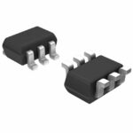 PBLS1502Y,115
The activity of extra discounts on wholesale prices is in full swing…
Please fill in your contact information and we will send you the latest wholesale price list.




