ChipApex | Global Electronic Components Supplier
SEARCH
Search Product
Search Post
— IC芯片 | 连接器 | 传感器 | 被动器件 —
Search productSearch post
— IC芯片 | 连接器 | 传感器 | 被动器件 —
Consult the customer manager about the wholesale price.
consultation hotline:86-132-6715-2157
email:[email protected]
Contact the product manager for consultation. One-stop consultation is available.
Do you want a lower wholesale price? Please send us your inquiry and we will reply immediately.
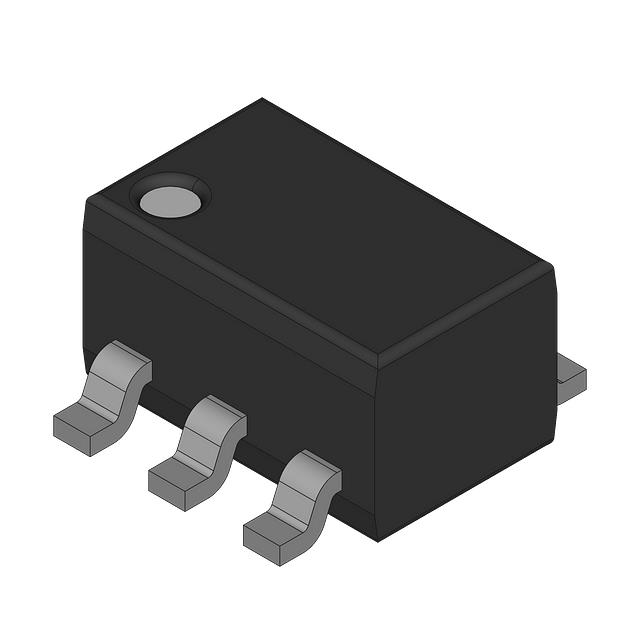
The PBLS1503Y is a dual-transistor component integrating a low VCEsat PNP BISS transistor and an NPN resistor-equipped transistor within a single SOT363 (SC-88) package. The PNP section supports a collector-emitter voltage of -15 V and a DC collector current up to -500 mA, with an equivalent on-resistance of 300 mΩ at full load. The NPN section provides a collector-emitter voltage of 50 V and a DC output current of 100 mA, featuring an integrated bias resistor of 10 kΩ. This configuration enables efficient high-side switching with minimal drive power requirements.
Verify the specific ordering suffix matches the required packing method, as the PBLS1503Y variant utilizes the SOT363 package available in tape and reel configurations. Confirm that the design accommodates the thermal resistance characteristics specified for the SC-88 plastic surface-mounted package under standard FR4 footprint conditions. Ensure input voltage limits for the NPN section are respected during operation.
Select this component when space constraints require combining a high-current PNP load switch with a signal or driver NPN transistor. The integrated bias resistor simplifies the NPN circuit design by eliminating external components. Verify that the -15 V rating of the PNP section aligns with the supply line voltage and that the 50 V rating of the NPN section suits the control signal levels.
This device belongs to Nexperia's portfolio of discrete semiconductor solutions, originally developed under the NXP Standard Product business. It is designed for automotive, industrial, computing, consumer, and wearable markets. The PBLS1503Y specifically addresses the need for compact, high-efficiency switching solutions in portable and battery-powered applications where board real estate is limited.
The datasheet lists PBLS1503V as a related part number sharing identical electrical specifications but housed in a different SOT666 package. Designers must verify pinout compatibility and physical footprint differences if substituting between the SOT363 and SOT666 variants.
The NPN transistor includes an integrated bias resistor (R1) with a typical value of 10 kΩ, which simplifies circuit design by reducing the need for external components.
The maximum DC collector current for the PNP transistor (TR1) is -500 mA.
The low VCEsat (BISS) technology minimizes voltage drop across the PNP transistor, thereby reducing power dissipation and improving efficiency in load switching applications.
 PBLS1503Y,115
The activity of extra discounts on wholesale prices is in full swing…
Please fill in your contact information and we will send you the latest wholesale price list.