 ChipApex | Global Electronic Components Supplier
SEARCH
Search Product
Search Post
— IC芯片 | 连接器 | 传感器 | 被动器件 —
Search productSearch post
— IC芯片 | 连接器 | 传感器 | 被动器件 —
Consult the customer manager about the wholesale price.
consultation hotline:86-132-6715-2157
email:[email protected]
Contact the product manager for consultation. One-stop consultation is available.
Do you want a lower wholesale price? Please send us your inquiry and we will reply immediately.
The PBLS1504V,115 is a dual-transistor load switch in an SOT666 surface-mounted package. It integrates a low VCEsat PNP transistor (TR1) and an NPN resistor-equipped transistor (TR2). TR1 provides a collector-emitter voltage of -15 V and DC collector current up to -500 mA with an equivalent on-resistance of 300 mΩ at -500 mA. TR2 offers a collector-emitter voltage of 50 V, DC output current of 100 mA, and a bias resistor of 22 kΩ. The device operates within an ambient temperature range of -65 °C to +150 °C.
Verify the specific ordering suffix
Select the PBLS1504V when an SOT666 package is required instead of the SOT363 variant. Ensure the design accommodates the -15 V limit for the PNP side and the 50 V limit for the NPN side. Verify thermal dissipation requirements against the 416 K/W junction-to-ambient resistance for the specific PCB footprint used.
This component belongs to the PBLS1504 series from NXP Semiconductors. It serves as a BISS (Bipolar Integrated Switch Solution) load switch. The PBLS1504V differs from the PBLS1504Y primarily by its SOT666 package format, while maintaining identical electrical characteristics and pinout functionality for system compatibility.
The PBLS1504Y is the functional equivalent using an SOT363 package. Verify footprint compatibility before substitution.
The NPN transistor includes an integrated bias resistor (typical value 22 kΩ) to facilitate switching control without requiring external base resistors.
The device features a low threshold voltage of less than 1 V, which is lower than typical MOSFET gate thresholds, allowing for easier drive from low-voltage logic.
The PNP transistor (TR1) supports a maximum DC collector current of -500 mA.
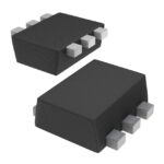 PBLS1504V,115
The activity of extra discounts on wholesale prices is in full swing…
Please fill in your contact information and we will send you the latest wholesale price list.




