 ChipApex | Global Electronic Components Supplier
SEARCH
Search Product
Search Post
— IC芯片 | 连接器 | 传感器 | 被动器件 —
Search productSearch post
— IC芯片 | 连接器 | 传感器 | 被动器件 —
Consult the customer manager about the wholesale price.
consultation hotline:86-132-6715-2157
email:[email protected]
Contact the product manager for consultation. One-stop consultation is available.
Do you want a lower wholesale price? Please send us your inquiry and we will reply immediately.
The PBLS1504Y-Q is a dual transistor load switch in a SOT363 package, containing a low VCEsat PNP transistor (TR1) and an NPN Resistor-Equipped Transistor (RET) (TR2). TR1 supports a collector current of -500 mA with a maximum collector-emitter voltage of -15 V. Its saturation resistance is typically 300 mΩ at -500 mA. TR2 provides an output current of 100 mA with a collector-emitter voltage of 50 V and includes an internal bias resistor R1 of 22 kΩ nominal. The device operates within a junction temperature range of -65 °C to 150 °C.
Verify the specific ordering suffix against the manufacturer's official documentation to confirm packaging details such as reel size or tape-and-reel specifications. Confirm that the component meets the required AEC-Q101 qualification status if intended for automotive deployment. Ensure the selected variant matches the exact pinout and marking code defined in the product data sheet.
Select this component when space constraints require integrating both a high-current PNP switch and a logic-compatible NPN RET into a single footprint. The integrated bias resistor on the NPN side simplifies circuit design by reducing external component count. Evaluate the thermal resistance characteristics relative to the expected ambient temperature and PCB copper area to ensure safe operation within the 150 °C junction limit.
This part belongs to Nexperia's PBLS series of loadswitch double transistors. It utilizes the SOT363 (SC-88) surface-mounted plastic package, which measures 2.1 mm x 1.25 mm x 0.95 mm. The series is designed to offer space-saving solutions for portable electronics and automotive systems requiring multiple switching functions.
Consult the Nexperia official cross-reference list for verified substitutes. Ensure any replacement maintains the SOT363 package dimensions and compatible electrical parameters for both the PNP and NPN sections.
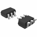 PBLS1504Y-QX
The activity of extra discounts on wholesale prices is in full swing…
Please fill in your contact information and we will send you the latest wholesale price list.




