 ChipApex | Global Electronic Components Supplier
SEARCH
Search Product
Search Post
— IC芯片 | 连接器 | 传感器 | 被动器件 —
Search productSearch post
— IC芯片 | 连接器 | 传感器 | 被动器件 —
Consult the customer manager about the wholesale price.
consultation hotline:86-132-6715-2157
email:[email protected]
Contact the product manager for consultation. One-stop consultation is available.
Do you want a lower wholesale price? Please send us your inquiry and we will reply immediately.
The PBLS4001Y,115 is a dual transistor assembly in an SOT363 (SC-88) package containing one PNP low VCEsat Breakthrough In Small Signal (BISS) transistor and one NPN Resistor-Equipped Transistor (RET). The PNP device supports a collector-emitter voltage of -40 V and a continuous collector current of -500 mA. The NPN RET features a collector-emitter voltage of 50 V, an output current of 100 mA, and a typical bias resistor of 2.2 kΩ. Total power dissipation is rated at 300 mW with a maximum junction temperature of 150 °C.
Verify the specific ordering suffix against the manufacturer's current documentation to confirm the packaging format and manufacturing origin. The standard tape and reel configuration utilizes an 8 mm pitch tape. Ensure compatibility with reflow soldering processes as specified in the thermal characteristics section of the datasheet.
Select this component when a mixed PNP/NPN load switch configuration is required in a minimal footprint. The PNP side is optimized for low saturation resistance, while the NPN side provides pre-biased switching capabilities. Confirm that the 40 V PNP and 50 V NPN voltage ratings align with the circuit requirements.
This part belongs to the Nexperia PBLS series of dual transistors designed for load switching applications. It integrates distinct transistor technologies within one SC-88 plastic surface-mounted package to minimize board space. The device replaces multiple discrete components, simplifying the bill of materials for portable and consumer electronics designs.
The PBLS4001V is the alternative variant housed in an SOT666 package. Verify pinout compatibility and physical dimensions before substituting, as the lead frame geometry differs between the SOT363 and SOT666 packages.
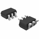 PBLS4001Y,115
The activity of extra discounts on wholesale prices is in full swing…
Please fill in your contact information and we will send you the latest wholesale price list.




