 ChipApex | Global Electronic Components Supplier
SEARCH
Search Product
Search Post
— IC芯片 | 连接器 | 传感器 | 被动器件 —
Search productSearch post
— IC芯片 | 连接器 | 传感器 | 被动器件 —
Consult the customer manager about the wholesale price.
consultation hotline:86-132-6715-2157
email:[email protected]
Contact the product manager for consultation. One-stop consultation is available.
Do you want a lower wholesale price? Please send us your inquiry and we will reply immediately.
The Nexperia PBSS4041SP,115 is a dual PNP Breakthrough In Small Signal (BISS) transistor housed in an SOT96-1 (SO8) surface-mount package. It features a collector-emitter voltage (VCEO) of -60 V and a continuous collector current (IC) of -5.9 A per transistor. The peak collector current (ICM) reaches -15 A for single pulses up to 1 ms. Key electrical characteristics include a maximum collector-base voltage (VCBO) of -60 V, an emitter-base voltage (VEBO) of -5 V, and a total power dissipation (Ptot) of 0.73 W at 25 °C ambient temperature on a standard FR4 PCB. The device operates within a junction temperature range of -55 °C to +150 °C.
Verify the specific ordering suffix
Select this component when a compact dual PNP solution with high current handling is required. The BISS technology offers superior performance over discrete transistors by reducing PCB area and improving thermal efficiency. Ensure the application stays within the absolute maximum ratings for collector current and power dissipation, particularly regarding thermal resistance on the chosen PCB layout.
This part belongs to the PBSS4041 series of low VCEsat BISS transistors from Nexperia. It serves as the PNP/PNP variant within the family, complementing the NPN/NPN version (PBSS4041SN). The series is designed to replace multiple discrete transistors in medium-power applications, offering integrated matching and reduced footprint through the SO8 plastic small outline package.
Direct functional equivalents within the same package and specification range should be sourced from Nexperia's BISS portfolio. Verify pinout compatibility and ensure that any substitute meets the -60 V voltage rating and -5.9 A current requirements. Cross-referencing with the PBSS4041SN may be necessary if an NPN configuration is acceptable.
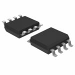 PBSS4041SP,115
The activity of extra discounts on wholesale prices is in full swing…
Please fill in your contact information and we will send you the latest wholesale price list.





