ChipApex | Global Electronic Components Supplier
SEARCH
Search Product
Search Post
— IC芯片 | 连接器 | 传感器 | 被动器件 —
Search productSearch post
— IC芯片 | 连接器 | 传感器 | 被动器件 —
Consult the customer manager about the wholesale price.
consultation hotline:86-132-6715-2157
email:[email protected]
Contact the product manager for consultation. One-stop consultation is available.
Do you want a lower wholesale price? Please send us your inquiry and we will reply immediately.
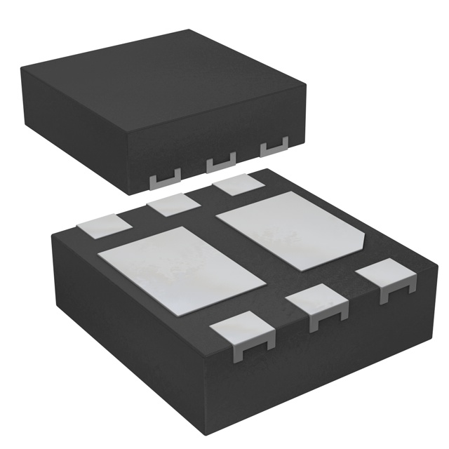
The PBSS5160PAP,115 is a PNP/PNP low VCEsat Breakthrough In Small Signal (BISS) transistor manufactured by Nexperia. It is housed in a leadless DFN2020-6 (SOT1118) surface-mounted device plastic package with dimensions of 2 x 2 x 0.65 mm. The component features a collector-emitter voltage (VCEO) of -60 V and a continuous collector current (IC) of -1 A, with a peak collector current (ICM) of -1.5 A for single pulses up to 1 ms. Key electrical characteristics include a typical DC current gain (hFE) ranging from 70 to 245 and a transition frequency (fT) of 125 MHz. The device operates within an ambient temperature range of -55 °C to +150 °C and is qualified under the AEC-Q101 standard.
Verify the specific ordering suffix
Select this component when a dual PNP configuration is required in a minimal footprint. The BISS technology ensures low saturation voltage, which minimizes power loss and heat generation compared to standard small-signal transistors. Ensure the PCB layout accommodates the DFN2020-6 thermal pad for optimal heat dissipation, as power derating curves vary significantly based on copper area and layer count.
This part belongs to Nexperia's BISS transistor family, designed for low-voltage, high-efficiency switching. It serves as the PNP/PNP complement to the NPN/NPN PBSS4160PAN and the NPN/PNP PBSS4160PA. The marking code for this device is '2L'.
Direct pin-compatible replacements within the same package are not explicitly listed in the provided documentation. Designers should evaluate the PBSS5160T-QR for single-transistor applications or other BISS series parts if dual configurations are needed, verifying electrical parameters against the original design requirements.
 PBSS5160PAP,115
The activity of extra discounts on wholesale prices is in full swing…
Please fill in your contact information and we will send you the latest wholesale price list.