 ChipApex | Global Electronic Components Supplier

SEARCH
Search Product
Search Post
— IC芯片 | 连接器 | 传感器 | 被动器件 —
Search productSearch post
— IC芯片 | 连接器 | 传感器 | 被动器件 —
Consult the customer manager about the wholesale price.
consultation hotline:86-132-6715-2157
email:[email protected]
Contact the product manager for consultation. One-stop consultation is available.
Do you want a lower wholesale price? Please send us your inquiry and we will reply immediately.
PCA2125TS/1,112 is listed in the Real Time Clock range at ChipApex. The manufacturer field lists NXP USA Inc.. Its product description is IC RTC CLK/CALENDAR SPI 14TSSOP. Review the specifications below when checking this part for your BOM.
The PCA2125TS/1,112 is a CMOS real-time clock and calendar optimized for low-power consumption. It operates within a voltage range of 1.3 V to 5.5 V and supports an operating temperature up to 125 °C. Data transfer occurs via a Serial Peripheral Interface (SPI) bus with a maximum data rate of 6.0 Mbit/s. The device provides year, month, day, weekday, hours, minutes, and seconds based on a 32.768 kHz quartz crystal. It features a typical backup current of 0.55 μA at VDD = 3.0 V and Tamb = 25 °C. The component is AEC Q100 qualified for automotive applications.
Verify the specific ordering suffix /1,112 against manufacturer documentation to confirm packaging details. Confirm availability status as distribution listings may indicate discontinued or limited stock conditions. Ensure compatibility with system voltage requirements ranging from 1.3 V to 5.5 V before procurement.
Select this component for applications requiring low-power RTC functionality with SPI interface. Ensure the design accommodates the TSSOP14 package dimensions. Verify that the system can handle the 32.768 kHz external crystal requirement. Check if AEC Q100 qualification is necessary for the target environment.
The PCA2125 is part of NXP Semiconductors' real-time clock family. The TS/1,112 designation indicates the TSSOP14 plastic thin shrink small outline package variant. This specific model is designed for high-temperature operation and automotive reliability standards.
Public confirmed substitute part numbers are not available in the provided source material. Consult NXP Semiconductors for direct replacements or cross-reference options based on pinout and electrical specifications.
The maximum data rate for the Serial Peripheral Interface (SPI) bus is 6.0 Mbit/s.
The alarm flag bit AF must be cleared by software writing a logic 0 to the corresponding bit in the Control_2 register.
The typical backup current is 0.55 μA when VDD is 3.0 V and the ambient temperature is 25 °C.
Explore related parts through Clock/Timing, Integrated Circuits (ICs), all product categories, ChipApex homepage.
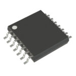 PCA2125TS/1,112

The activity of extra discounts on wholesale prices is in full swing…
Please fill in your contact information and we will send you the latest wholesale price list.





