 ChipApex | Global Electronic Components Supplier

SEARCH
Search Product
Search Post
— IC芯片 | 连接器 | 传感器 | 被动器件 —
Search productSearch post
— IC芯片 | 连接器 | 传感器 | 被动器件 —
Consult the customer manager about the wholesale price.
consultation hotline:86-132-6715-2157
email:[email protected]
Contact the product manager for consultation. One-stop consultation is available.
Do you want a lower wholesale price? Please send us your inquiry and we will reply immediately.
PCA9512D,118 is listed in the Signal Buffers, Repeaters, Splitters range at ChipApex. The manufacturer field lists NXP USA Inc.. Its product description is IC BUFFER I2C/SMBUS HOTSWAP 8SO. Review the specifications below when checking this part for your BOM.
The PCA9512D,118 is a hot swappable I2C and SMBus buffer manufactured by NXP Semiconductors. It provides bidirectional buffering for SDA and SCL lines to prevent signal corruption during live board insertion in multi-point backplane systems. The device features two dedicated supply voltage pins (VCC and VCC2) supporting level shifting between 3.3 V and 5 V systems within an operating range of 2.7 V to 5.5 V. It includes ∆V/∆t rise time accelerators with hardware disable capability via the ACC pin, supports clock stretching, and offers ESD protection exceeding 2000 V HBM. The component operates at frequencies up to 400 kHz and is available in SO8 packages.
Verify the ordering suffix '118' against current manufacturer documentation to confirm specific packaging details. Confirm that the SO8 package designation aligns with your PCB footprint requirements. Ensure compatibility with the specified -40 °C to +85 °C temperature range for your intended application environment before finalizing procurement.
Select this component when designing systems requiring hot swapping capabilities for I/O cards without disrupting active bus operations. It is suitable for applications needing robust level translation between 3.3 V and 5 V logic levels. Consider the ACC pin configuration if system loading requires disabling the internal rise time accelerators to optimize performance for specific bus capacitance conditions.
The PCA9512 belongs to the Philips/NXP PCA951x series of I2C bus buffers. Unlike the PCA9510 which lacks accelerators, or the PCA9513/14 which include current sources, the PCA9512 specifically targets dual-supply level shifting with configurable acceleration. It complements the PCA9511 by adding the ACC pin for accelerator control and dual VCC pins for improved noise margin in mixed-voltage environments.
Publicly confirmed substitute part numbers are not provided in the source material. Designers should evaluate other members of the PCA951x family, such as the PCA9511 or PCA9513, based on specific feature requirements like accelerator control or current sourcing capabilities.
The device enters an under-voltage lockout state until both VCC and VCC2 exceed 2.5 V. During initialization, it activates a 1 V precharge circuitry before enabling connection circuitry upon detecting a stop bit or bus idle condition.
The ACC pin is a digital input that enables or disables the rise-time accelerators on all SDA and SCL pins. Driving it to VCC2 enables normal operation, while connecting it to GND turns off the accelerators for lightly loaded systems.
Yes, the dynamic offset design allows connection to other PCA9510/11/12/13/14 devices in series or parallel. However, manufacturers generally recommend limiting series connections to two buffers to avoid excessive offset voltage accumulation.
Explore related parts through Interface, Integrated Circuits (ICs), all product categories, ChipApex homepage.
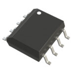 PCA9512D,118

The activity of extra discounts on wholesale prices is in full swing…
Please fill in your contact information and we will send you the latest wholesale price list.





