 ChipApex | Global Electronic Components Supplier

SEARCH
Search Product
Search Post
— IC芯片 | 连接器 | 传感器 | 被动器件 —
Search productSearch post
— IC芯片 | 连接器 | 传感器 | 被动器件 —
Consult the customer manager about the wholesale price.
consultation hotline:86-132-6715-2157
email:[email protected]
Contact the product manager for consultation. One-stop consultation is available.
Do you want a lower wholesale price? Please send us your inquiry and we will reply immediately.
PCA9519PW,112 is listed in the Signal Buffers, Repeaters, Splitters range at ChipApex. The manufacturer field lists NXP USA Inc.. Its product description is IC REDRIVER I2C 4CH 20TSSOP. Review the specifications below when checking this part for your BOM.
The PCA9519PW,112 is a 4-channel level translating I2C-bus/SMBus repeater manufactured by NXP Semiconductors. It enables low-voltage processors to interface with standard I2C or SMBus I/O devices while retaining all system operating modes. The device provides bidirectional buffering for data (SDA) and clock (SCL) lines, allowing up to 400 pF capacitance on the higher voltage side. Port A operates at 1.0 V to VCC(B) - 1.5 V, while Port B operates at 3.0 V to 5.5 V. It supports clock frequencies from 0 Hz to 400 kHz, features an active HIGH enable pin, and includes a 50 ns glitch filter on the B-side input.
Verify the specific ordering suffix against the manufacturer's latest documentation to confirm package type and packing method. The datasheet indicates that the PW variant is typically available in reel pack configurations. Ensure compatibility with the required temperature range of -40 °C to +85 °C before finalizing procurement specifications.
Select this component when interfacing low-voltage logic (down to 1.0 V) with standard 3.3 V or 5 V I2C peripherals. It is suitable for applications requiring isolation of bus capacitance or connection of multiple masters. Ensure the design accounts for ground offset limitations on Port A to prevent signal recognition errors during low-level transitions.
The PCA9519 belongs to NXP's family of I2C-bus and SMBus interface buffers and repeaters. It is designed to facilitate communication between systems operating at different voltage levels. The PW suffix denotes the TSSOP20 plastic thin shrink small outline package, which is one of the two primary package options offered for this device series alongside the HVQFN24.
Public confirmed substitute part numbers are not provided in the source material. Designers should consult the official NXP website for the most current product status and potential obsolescence notices regarding this specific model number.
No, Port A utilizes an internal 1 mA current source for pull-up, eliminating the need for external pull-up resistors on the lower voltage side.
The device allows a maximum capacitance of 400 pF on Port B due to its bidirectional buffering capabilities.
Port A uses a current sensing mechanism to detect LOW signals, which prevents bus lock-up. Additionally, the output pull-down on Port A is set to approximately 0.2 V to ensure proper signal recognition.
Explore related parts through Interface, Integrated Circuits (ICs), all product categories, ChipApex homepage.
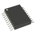 PCA9519PW,112

The activity of extra discounts on wholesale prices is in full swing…
Please fill in your contact information and we will send you the latest wholesale price list.





