 ChipApex | Global Electronic Components Supplier
SEARCH
Search Product
Search Post
— IC芯片 | 连接器 | 传感器 | 被动器件 —
Search productSearch post
— IC芯片 | 连接器 | 传感器 | 被动器件 —
Consult the customer manager about the wholesale price.
consultation hotline:86-132-6715-2157
email:[email protected]
Contact the product manager for consultation. One-stop consultation is available.
Do you want a lower wholesale price? Please send us your inquiry and we will reply immediately.
The Microchip Technology PCI11101/MXX is a single-chip PCIe switch integrating a USB 3.2 Gen 2 host controller and programmable I/O. It features a 4-lane (4x8GT/s) upstream port and a 2-lane (2x8GT/s) downstream port, certified for PCIe Gen 4 compliance. The device includes an integrated xHCI USB 3.2 Gen 2 host controller with 10Gbps PHY support. Power requirements are met by two external supplies: +3.3V and +1.1V. It operates within commercial (0°C to +70°C) or industrial (-40°C to +85°C) temperature ranges and is housed in a 132-pin DRQFN package.
Verify the ordering suffix against the product identification system. The 'Blank' suffix indicates standard tray packaging, while 'T' denotes tape and reel. Temperature grades are specified as 'Blank' for commercial (0°C to +70°C) or 'I' for industrial (-40°C to +85°C). Confirm the specific variant matches the required environmental and packaging specifications for the design.
Select the PCI11101/MXX when high-bandwidth PCIe subsystems are required for embedded applications. Ensure the design accommodates the 132-pin DRQFN package dimensions and land pattern. Verify that the system architecture supports the necessary clocking (single-ended 25MHz crystal/clock plus PCIe reference) and power rails (+3.3V, +1.1V) before finalizing the component choice.
The PCI11101 belongs to Microchip's specialized interface IC portfolio, designed to consolidate connectivity functions. It combines switching, host control, and programmable I/O into a single silicon solution, reducing bill of materials complexity compared to discrete implementations. This integration targets modern embedded architectures requiring flexible I/O mapping and high-speed data transfer capabilities.
Publicly confirmed substitute part numbers are not available in the provided documentation. Designers should consult Microchip sales offices for alternative components or updated product family recommendations if the PCI11101/MXX is no longer suitable for the application.
The device supports a maximum line rate of 8GT/s and is certified against the GEN4 compliance program defined in the PCIe Revision 4.x specifications.
Although multiple internal clocks are generated by an integrated clock farm, only a single-ended 25MHz clock or crystal and a PCIe reference clock are required externally.
Yes, the latch-up performance exceeds 150mA per EIA/JESD78, Class II standards.
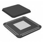 PCI11101/MXX
The activity of extra discounts on wholesale prices is in full swing…
Please fill in your contact information and we will send you the latest wholesale price list.





