 ChipApex | Global Electronic Components Supplier

SEARCH
Search Product
Search Post
— IC芯片 | 连接器 | 传感器 | 被动器件 —
Search productSearch post
— IC芯片 | 连接器 | 传感器 | 被动器件 —
Consult the customer manager about the wholesale price.
consultation hotline:86-132-6715-2157
email:[email protected]
Contact the product manager for consultation. One-stop consultation is available.
Do you want a lower wholesale price? Please send us your inquiry and we will reply immediately.
PCK351DB,118 is listed in the Clock Buffers, Drivers range at ChipApex. The manufacturer field lists NXP USA Inc.. Its product description is IC CLK BUFFER 1:10 125MHZ 24SSOP. Review the specifications below when checking this part for your BOM.
The PCK351DB,118 is a high-performance 3.3 V LVTTL clock distribution device featuring one input and ten outputs with three-state capability. It operates within a supply voltage range of 3.0 V to 3.6 V and supports an industrial temperature range of −40 °C to +85 °C. The component utilizes distributed VCC and GND pins to minimize switching noise. Key electrical parameters include a propagation delay (tPLH/tPHL) of 2.5 ns to 5.9 ns, output skew time (tsk(o)) up to 0.5 ns, and pulse skew time (tsk(p)) up to 0.8 ns under recommended operating conditions. It provides balanced high-drive outputs with -32 mA IOH and 32 mA IOL capabilities.
Verify the ordering suffix '118' against current manufacturer documentation to confirm specific tape-and-reel packaging or moisture sensitivity level requirements. Ensure the source document matches the requested part number variant before finalizing procurement decisions.
Select this component for designs requiring a single clock source to drive ten loads with minimal skew. Ensure the system operates between 3.0 V and 3.6 V. Verify that the load capacitance does not exceed 50 pF per output to maintain specified dynamic characteristics. Unused pins must be tied HIGH or LOW.
The PCK351DB variant specifically denotes the SSOP24 package (SOT340-1), which is a plastic shrink small outline package with 24 leads and a body width of 5.3 mm. This differs from the SO24 (SOT137-1) version. Both variants share identical electrical specifications and functionality.
Public confirmed substitute part numbers are not available in the provided datasheet.
Explore related parts through Clock/Timing, Integrated Circuits (ICs), all product categories, ChipApex homepage.
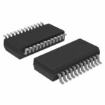 PCK351DB,118

The activity of extra discounts on wholesale prices is in full swing…
Please fill in your contact information and we will send you the latest wholesale price list.






