ChipApex | Global Electronic Components Supplier
SEARCH
Search Product
Search Post
— IC芯片 | 连接器 | 传感器 | 被动器件 —
Search productSearch post
— IC芯片 | 连接器 | 传感器 | 被动器件 —
Consult the customer manager about the wholesale price.
consultation hotline:86-132-6715-2157
email:[email protected]
Contact the product manager for consultation. One-stop consultation is available.
Do you want a lower wholesale price? Please send us your inquiry and we will reply immediately.
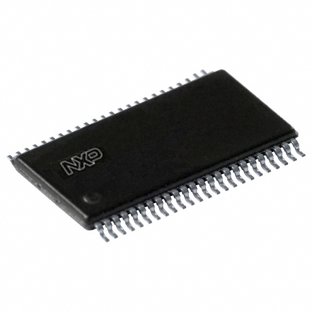
The PCKV857ADGV,112 is a differential clock driver and distribution device manufactured by NXP USA Inc. It operates within a frequency range of 100 MHz to 250 MHz and features a 1-to-10 output ratio. The component utilizes an integrated Phase-Locked Loop (PLL) to synchronize outputs via an external feedback pin. It accepts SSTL-2 differential inputs and provides ten pairs of SSTL_2 differential outputs. Power requirements include a VDDQ supply of 2.3 V to 2.7 V and an AVDD supply of 2.2 V to 2.7 V. The device is housed in a 48-TSSOP package with an operating temperature range of 0°C to +70°C.
Verify the specific ordering suffix '112' against official NXP documentation to confirm tape-and-reel packaging details. Confirm that the 48-TSSOP (SOT480-1) package variant matches the design requirements. Check for any superseded data sheets or engineering change notifications related to this part number before finalizing procurement plans.
Select this component when a 1:10 differential clock fan-out is required for SSTL_2 compliant memory systems. Ensure the design supports the 2.3 V to 2.7 V VDDQ supply voltage. Verify that the PCB layout accommodates the 48-pin TSSOP footprint and allows for proper thermal dissipation within the 0°C to +70°C operating range.
This device belongs to the Philips/NXP Semiconductors PCKV857 family of clock drivers. It supersedes earlier versions such as the PCKV857A without suffix or those with different packaging codes like DGG. The product data indicates it is designed to reduce signal loads on memory controllers and prevent waveform distortions in high-speed digital environments.
Publicly confirmed substitute part numbers are not available in the provided source material. Designers should consult NXP Semiconductors directly for cross-reference information or updated product line replacements.
 PCKV857ADGV,112
The activity of extra discounts on wholesale prices is in full swing…
Please fill in your contact information and we will send you the latest wholesale price list.