ChipApex | Global Electronic Components Supplier
SEARCH
Search Product
Search Post
— IC芯片 | 连接器 | 传感器 | 被动器件 —
Search productSearch post
— IC芯片 | 连接器 | 传感器 | 被动器件 —
Consult the customer manager about the wholesale price.
consultation hotline:86-132-6715-2157
email:[email protected]
Contact the product manager for consultation. One-stop consultation is available.
Do you want a lower wholesale price? Please send us your inquiry and we will reply immediately.
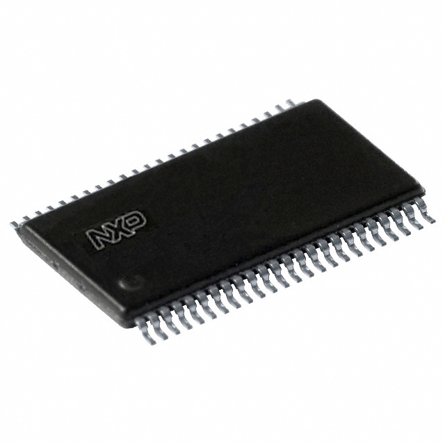
The PCKV857DGV,112 is a differential clock driver and distribution IC designed for DDR SDRAM applications. It features an integrated PLL to distribute a single differential SSTL_2 input clock to ten differential SSTL_2 output pairs. Operating within a frequency range of 70 MHz to 190 MHz, the device ensures signal integrity with very low skew (max 75 ps) and jitter (max 75 ps). It utilizes separate analog (AVDD) and digital (VDDQ) power supplies ranging from 2.3 V to 2.7 V. The component is housed in a 48-pin TSSOP package (SOT-480-1) and supports spread spectrum clocking for EMI reduction.
Verify the specific ordering suffix '112' against official NXP documentation, as standard datasheets list 'PCKV857DGV'. Confirm current product status, as related variants may be discontinued or superseded by newer revisions. Ensure supply chain sources provide valid traceability for this specific batch code.
Select this component when a 1:10 differential clock fan-out is required for SSTL_2 compliant DDR designs. Ensure the design accommodates separate AVDD and VDDQ power domains. Verify that the PCB layout supports the 48-TSSOP package dimensions and thermal requirements for the specified operating temperature range.
This part belongs to the PCKV857 family of zero-delay buffer clock drivers originally developed by Philips Semiconductors. The DGV suffix specifically denotes the 48-pin Plastic TSSOP (TVSOP) package variant. It serves as a critical interface between memory controllers and multiple DRAM modules in high-performance computing architectures.
Direct replacements include other PCKV857 package variants such as PCKV857DGG (standard TSSOP) or PCKV857EV (VFBGA), provided the mechanical footprint matches the design constraints. Cross-referencing with updated NXP product selection guides is recommended for availability.
 PCKV857DGV,112
The activity of extra discounts on wholesale prices is in full swing…
Please fill in your contact information and we will send you the latest wholesale price list.