ChipApex | Global Electronic Components Supplier
SEARCH
Search Product
Search Post
— IC芯片 | 连接器 | 传感器 | 被动器件 —
Search productSearch post
— IC芯片 | 连接器 | 传感器 | 被动器件 —
Consult the customer manager about the wholesale price.
consultation hotline:86-132-6715-2157
email:[email protected]
Contact the product manager for consultation. One-stop consultation is available.
Do you want a lower wholesale price? Please send us your inquiry and we will reply immediately.
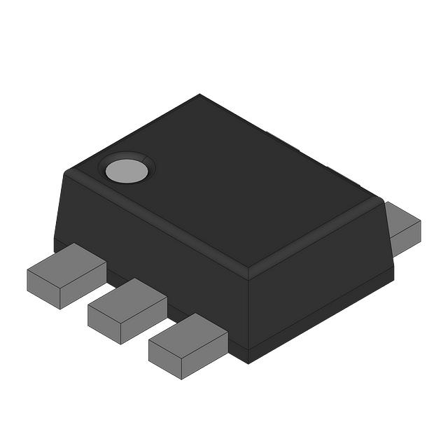
The PEMD12,115 is a dual pre-biased transistor array manufactured by Nexperia USA Inc., housed in an SOT-666 surface-mount package. It integrates one NPN and one PNP bipolar junction transistor (BJT) with built-in biasing resistors. The device supports a maximum collector-emitter voltage of 50V and a continuous collector current of 100mA. Each internal transistor includes a 47 kΩ base resistor (R1) and a 47 kΩ emitter resistor (R2). Key electrical characteristics include a DC current gain (hFE) of at least 80 at 5mA/5V for the NPN and 60 at 5mA/5V for the PNP, with a maximum saturation voltage of 150mV at low currents. The unit operates within a temperature range of -55°C to +150°C and has a maximum power dissipation of 300mW.
Verify the specific ordering suffix and manufacturing date code upon receipt to ensure compliance with project requirements. Confirm that the received components match the SOT-666 package dimensions and pinout configuration specified in the official datasheet. Check for physical integrity and absence of contamination before soldering.
Select this component when a design requires both NPN and PNP switching functions in a minimal footprint. The integrated 47kΩ resistors reduce external component count compared to using discrete transistors. Ensure the required current gain and saturation voltage meet the load specifications, as these values are optimized for general-purpose digital switching rather than linear amplification.
This part belongs to Nexperia's portfolio of pre-biased transistor arrays designed to replace multiple discrete components. The SOT-666 package allows for automated placement in dense PCB layouts. It serves as a direct replacement for similar dual BJT arrays from other manufacturers, offering standardized performance for common-mode noise immunity and signal inversion tasks.
Check pin-to-pin compatibility with existing designs using alternative dual BJT arrays. Verify that substitute parts offer equivalent hFE and Vce(sat) specifications. Ensure the replacement package matches the SOT-666 footprint to avoid rework or redesign efforts.
The device includes a 47kΩ base resistor (R1) and a 47kΩ emitter resistor (R2) for each transistor. These resistors provide biasing and improve switching stability, reducing the need for external components.
No, it is designed primarily for digital switching applications. The specified parameters, such as saturation voltage and current gain, are optimized for on/off states rather than linear operation.
The maximum power dissipation is 300mW. This limit must not be exceeded under any operating conditions to prevent thermal damage to the device.
 PEMD12,115
The activity of extra discounts on wholesale prices is in full swing…
Please fill in your contact information and we will send you the latest wholesale price list.