 ChipApex | Global Electronic Components Supplier

SEARCH
Search Product
Search Post
— IC芯片 | 连接器 | 传感器 | 被动器件 —
Search productSearch post
— IC芯片 | 连接器 | 传感器 | 被动器件 —
Consult the customer manager about the wholesale price.
consultation hotline:86-132-6715-2157
email:[email protected]
Contact the product manager for consultation. One-stop consultation is available.
Do you want a lower wholesale price? Please send us your inquiry and we will reply immediately.
PI49FCT3805HE is listed in the Clock Buffers, Drivers range at ChipApex. The manufacturer field lists Diodes Incorporated. Its product description is IC CLK BUFFER 1:5 50MHZ 20SSOP. Review the specifications below when checking this part for your BOM.
The PI49FCT3805HE is a 3.3V non-inverting clock driver manufactured by Diodes Incorporated, housed in a 20-pin SSOP package with a 209-mil width. It features two independent buffer groups, each providing a 1-to-5 fanout configuration with active LOW 3-state output enable inputs (OEA, OEB). The device operates within a supply voltage range of 3.0V to 3.6V and supports an industrial temperature range of -40°C to +85°C. Key electrical specifications include a maximum propagation delay of 6.5ns at 50pF load, extremely low output skew of 0.7ns, and typical quiescent power consumption of 1mW.
Verify the 'E' suffix indicates Pb-free and Green compliant packaging as specified in the ordering information table. Confirm the 'H' package code corresponds to the 20-pin 209-mil wide SSOP form factor. Ensure the required speed grade matches the Blank designation for standard performance characteristics.
Select this component when a non-inverting clock driver with dual 1:5 fanouts is required. The PI49FCT3805HE provides TTL-compatible inputs and CMOS outputs suitable for mixed-signal environments. Consider the 0.7ns max skew and 6.5ns max propagation delay for timing-critical high-speed applications operating at 3.3V.
This part belongs to the PI49FCT3805/3806 series of 3.3V Fast CMOS Buffer/Clock Drivers. It serves as the non-inverting counterpart to the PI49FCT3806. The HE variant specifically denotes the Pb-free and Green packaging option within the H (SSOP) package family.
Public confirmed substitute part numbers are not available in the provided source material.
The MON pin serves as a monitor output pin, providing a signal identical to the other outputs for diagnostic purposes.
The device has two independent groups of buffers, each with its own Output Enable input (OEA or OEB). These inputs are active LOW; when HIGH, the respective outputs enter a high-impedance state.
The device features hysteresis on all inputs, with a typical value of 150 mV.
Explore related parts through Clock/Timing, Integrated Circuits (ICs), all product categories, ChipApex homepage.
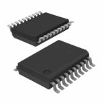 PI49FCT3805HE

The activity of extra discounts on wholesale prices is in full swing…
Please fill in your contact information and we will send you the latest wholesale price list.





