 ChipApex | Global Electronic Components Supplier

SEARCH
Search Product
Search Post
— IC芯片 | 连接器 | 传感器 | 被动器件 —
Search productSearch post
— IC芯片 | 连接器 | 传感器 | 被动器件 —
Consult the customer manager about the wholesale price.
consultation hotline:86-132-6715-2157
email:[email protected]
Contact the product manager for consultation. One-stop consultation is available.
Do you want a lower wholesale price? Please send us your inquiry and we will reply immediately.
PI6C10806BLEX is listed in the Clock Buffers, Drivers range at ChipApex. The manufacturer field lists Diodes Incorporated. Its product description is IC CLK BUFFER 1:6 160MHZ 16TSSOP. Review the specifications below when checking this part for your BOM.
The PI6C10806BLEX is a low skew, six-output crystal oscillator driver manufactured by Diodes Incorporated. It supports operating voltages of 1.5V, 1.8V, 2.5V, and 3.3V with an input frequency range of 10MHz to 50MHz using a crystal, or up to 160MHz when driven by an external clock source. The device features output-to-output skew of less than 80ps and synchronous output enables. It is housed in a 16-pin TSSOP package and operates within an industrial temperature range of –40°C to +85°C.
Verify the 'X' suffix indicates Tape/Reel packaging rather than tube. Confirm the component meets specific environmental requirements such as lead-free and halogen-free standards if required by the design. Ensure the supply voltage matches the selected VDD/VDDO configuration for optimal performance.
Select this component for applications requiring a 1:6 fan-out from a crystal or external clock source. Ensure the load capacitance matches the crystal specifications (typically 18pF). Verify that the output voltage level (VDDO) aligns with the receiving logic inputs across the full industrial temperature range.
The PI6C10806BLEX belongs to the PI6C10806B series of clock buffers. It is designed for low power and high frequency applications. The 'L' denotes the 16-pin TSSOP package, 'E' indicates lead-free/green status, and 'X' specifies tape and reel packaging.
Check for direct pin-compatible replacements within the PI6C10806B family. Verify that any substitute maintains the same 1:6 output ratio, low skew characteristics, and compatible voltage ranges.
The maximum switching frequency is 160 MHz when driven by an external clock source. When using a crystal, the frequency is limited to 50 MHz.
The device has two synchronous output enable inputs, ENABLE1 and ENABLE2. They control two groups of outputs: one group of five outputs and one single output.
At 25MHz with an integration range of 100Hz to 1MHz, the typical RMS random phase jitter varies by voltage: 0.098 ps at 3.3V, 0.112 ps at 2.5V, 0.233 ps at 1.8V, and 0.277 ps at 1.5V.
Explore related parts through Clock/Timing, Integrated Circuits (ICs), all product categories, ChipApex homepage.
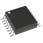 PI6C10806BLEX

The activity of extra discounts on wholesale prices is in full swing…
Please fill in your contact information and we will send you the latest wholesale price list.





