 ChipApex | Global Electronic Components Supplier

SEARCH
Search Product
Search Post
— IC芯片 | 连接器 | 传感器 | 被动器件 —
Search productSearch post
— IC芯片 | 连接器 | 传感器 | 被动器件 —
Consult the customer manager about the wholesale price.
consultation hotline:86-132-6715-2157
email:[email protected]
Contact the product manager for consultation. One-stop consultation is available.
Do you want a lower wholesale price? Please send us your inquiry and we will reply immediately.
PI6C10810LEX is listed in the Clock Buffers, Drivers range at ChipApex. The manufacturer field lists Diodes Incorporated. Its product description is IC CLK BUF 1:10 250MHZ 20TSSOP. Review the specifications below when checking this part for your BOM.
The PI6C10810LEX is a high-speed, low-noise, non-inverting split 1-to-10 clock buffer manufactured by Diodes Incorporated. It supports supply voltages of 1.2V, 1.5V, 1.8V, or 2.5V across three independent banks (A, B, and C). The device achieves a maximum frequency of 250 MHz at 2.5V, with output-to-output skew as low as 60 ps in Bank A. It features low propagation delay (<2.0 ns at 2.5V) and additive jitter of 50 ps. Packaged in a 20-pin TSSOP (L20), it operates within an industrial temperature range of -40°C to 85°C.
Verify the 'LEX' suffix against official documentation to confirm the specific package variant and tape/reel configuration. Confirm current availability status as older Pericom/Diodes products may have discontinuation notices. Ensure compatibility with existing PCB footprint for the 20-TSSOP package.
Select based on required supply voltage per bank (1.2V, 1.5V, 1.8V, or 2.5V) to meet system timing constraints. Consider the split-bank architecture if different output voltage domains are needed. Verify that the 250 MHz max frequency meets the target application's clock speed requirements.
The PI6C10810 series was originally developed by Pericom Semiconductor Corporation before being acquired by Diodes Incorporated. The 'LE' designation indicates a lead-free and green RoHS-compliant version in a 20-pin TSSOP package. The 'X' suffix typically denotes tape and reel packaging.
Check for direct replacements within the Diodes Incorporated portfolio such as the PI6C10810HE (SSOP) or PI6C10810QE (QSOP) if package changes are acceptable. Verify pinout compatibility and electrical specifications before substitution.
The maximum input frequency is up to 250 MHz when powered at 2.5V.
Output-to-output skew is <60 ps in Bank A (CLK0-CLK4) at 2.5V, <30 ps in Bank C (CLK5-CLK6), and <150 ps in Bank B (CLK7-CLK9).
Yes, Bank A, Bank B, and Bank C can be powered independently at 1.2V, 1.5V, 1.8V, or 2.5V.
Explore related parts through Clock/Timing, Integrated Circuits (ICs), all product categories, ChipApex homepage.
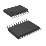 PI6C10810LEX

The activity of extra discounts on wholesale prices is in full swing…
Please fill in your contact information and we will send you the latest wholesale price list.





