 ChipApex | Global Electronic Components Supplier
SEARCH
Search Product
Search Post
— IC芯片 | 连接器 | 传感器 | 被动器件 —
Search productSearch post
— IC芯片 | 连接器 | 传感器 | 被动器件 —
Consult the customer manager about the wholesale price.
consultation hotline:86-132-6715-2157
email:[email protected]
Contact the product manager for consultation. One-stop consultation is available.
Do you want a lower wholesale price? Please send us your inquiry and we will reply immediately.
The PI6C20400BLE is a PCIe 3.0 compliant high-speed, low-noise differential clock buffer designed as a companion to PCIe 3.0 clock generators. It distributes the differential SRC clock from a source generator to four pairs of differential clock outputs in either PLL or bypass mode. The device operates on a single 3.3V supply with an input frequency range of 100 MHz to 400 MHz in bypass mode and up to 105 MHz in PLL mode. It features low skew and jitter characteristics, SMBus control for output enablement and power-down states, and is housed in a 28-pin TSSOP package.
Verify the ordering suffix 'LE' corresponds to the 28-pin TSSOP (L28) package variant. Confirm RoHS compliance and Pb-free status as specified in the datasheet. Ensure the application circuit matches the recommended test load configuration (Rs = 33Ω, Rp = 49.9Ω) for accurate performance validation.
Select this component when a 1:4 differential clock fan-out with integrated phase-locked loop filtering is required for PCIe applications. Choose the PLL mode for frequencies up to 105 MHz if jitter filtering is needed, or use the bypass mode for frequencies between 100 MHz and 400 MHz. Ensure the design supports the required 3.3V supply voltage and provides adequate thermal dissipation for the TSSOP package.
The PI6C20400B series includes variants with different packaging options. The 'HE' suffix denotes the 28-pin SSOP package, while the 'LE' suffix indicates the 28-pin TSSOP package. Adding an 'X' suffix to either code specifies tape and reel packaging. All variants share identical electrical characteristics and functionality.
Publicly confirmed substitute part numbers are not available in the provided documentation.
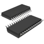 PI6C20400BLE
The activity of extra discounts on wholesale prices is in full swing…
Please fill in your contact information and we will send you the latest wholesale price list.






