 ChipApex | Global Electronic Components Supplier
SEARCH
Search Product
Search Post
— IC芯片 | 连接器 | 传感器 | 被动器件 —
Search productSearch post
— IC芯片 | 连接器 | 传感器 | 被动器件 —
Consult the customer manager about the wholesale price.
consultation hotline:86-132-6715-2157
email:[email protected]
Contact the product manager for consultation. One-stop consultation is available.
Do you want a lower wholesale price? Please send us your inquiry and we will reply immediately.
The PI6C20800SIAE is a PCI Express differential clock buffer manufactured by Diodes Incorporated. It provides one-to-eight fanout of differential HCSL clocks with an integrated programmable PLL for jitter filtering. The device operates on a single 3.3V supply within the 3.135V to 3.465V range and supports frequencies up to 400MHz in bypass mode. Designed for industrial applications, it functions between -40°C and +85°C. The component utilizes a 48-pin TSSOP package (6.10mm width) and includes SMBus control for output enablement and power management.
Verify the specific suffix 'AE' confirms the 48-pin TSSOP package and industrial temperature grade (-40°C to +85°C). Confirm RoHS compliance status via the manufacturer's documentation before integration. Check current availability as this component may be subject to end-of-life notifications or discontinuation.
Select the PI6C20800SIAE when industrial temperature operation is required alongside low skew performance. Ensure the design accommodates the 48-TSSOP footprint. Verify that the host system requires SMBus-based output control and that the 3.3V logic levels are compatible with the driving circuitry.
This part belongs to the PI6C20800S family of high-speed, low-noise differential clock buffers. The 'I' suffix denotes the industrial temperature variant, while 'A' specifies the TSSOP package. It serves as a companion to the PI6C410BS clock generator for Intel server chipsets.
The PI6C20800SVE is the commercial temperature equivalent in the same package. For tape and reel packaging, consider the PI6C20800SIAEX variant. No direct cross-manufacturer substitutes are verified in the provided data.
Asserting the PWRDWN# pin forces all outputs into a tristate condition and reduces power consumption. During this state, SDA and SCLK inputs must also be tristated.
The device supports a maximum SRC/SRC# input frequency of 400 MHz when operating in bypass mode.
Yes, the input frequency can be divided by two by pulling the SRC_DIV# pin LOW.
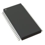 PI6C20800SIAE
The activity of extra discounts on wholesale prices is in full swing…
Please fill in your contact information and we will send you the latest wholesale price list.






