 ChipApex | Global Electronic Components Supplier
SEARCH
Search Product
Search Post
— IC芯片 | 连接器 | 传感器 | 被动器件 —
Search productSearch post
— IC芯片 | 连接器 | 传感器 | 被动器件 —
Consult the customer manager about the wholesale price.
consultation hotline:86-132-6715-2157
email:[email protected]
Contact the product manager for consultation. One-stop consultation is available.
Do you want a lower wholesale price? Please send us your inquiry and we will reply immediately.
The PI6C21200AE is a high-speed, low-noise PCIe differential clock buffer designed for Intel chipsets. It distributes twelve pairs of HCSL-compatible differential clocks with a maximum frequency of 400 MHz. The device supports a 3.3V supply voltage (3.135V to 3.465V) and operates within a commercial temperature range of 0°C to 70°C. Key electrical parameters include output-to-output skew less than 50 ps and cycle-to-cycle jitter under 50 ps. It features programmable PLL bandwidth, gear ratios, and individual output enable controls via hardware pins or SMBus interface.
Verify the 'AE' suffix indicates a Pb-Free and Green package in the 56-pin TSSOP format. Confirm that the specific revision matches the required thermal and mechanical specifications for the target PCB layout. Ensure compatibility with the intended SMBus controller protocol for configuration.
Select this component when a 1:12 fan-out ratio is required for PCIe reference clocks. It is suitable for systems needing programmable gear ratios to support various CPU input frequencies. Verify that the 0°C to 70°C operating range meets the environmental requirements of the application.
This part belongs to the PI6C21xxx series of PCIe clock buffers. It is typically paired with synthesizers like the PI6C410B to provide complete clock generation solutions for complex chipset architectures requiring multiple synchronized differential clock domains.
Check datasheets for other PI6C21xxx variants (e.g., different pin counts or ratios) if the 1:12 configuration does not match the design needs. Ensure any substitute maintains the same HCSL signaling standard and SMBus compatibility.
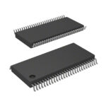 PI6C21200AE
The activity of extra discounts on wholesale prices is in full swing…
Please fill in your contact information and we will send you the latest wholesale price list.






