 ChipApex | Global Electronic Components Supplier
SEARCH
Search Product
Search Post
— IC芯片 | 连接器 | 传感器 | 被动器件 —
Search productSearch post
— IC芯片 | 连接器 | 传感器 | 被动器件 —
Consult the customer manager about the wholesale price.
consultation hotline:86-132-6715-2157
email:[email protected]
Contact the product manager for consultation. One-stop consultation is available.
Do you want a lower wholesale price? Please send us your inquiry and we will reply immediately.
The PI6C2410LE is a low skew, low jitter PLL clock buffer with divider or multiplier capabilities, designed for PCI-X applications in servers and workstations. It features four synchronous outputs synchronized to the input and each other. The device supports selectable input frequency ranges of 10-40 MHz and 40-80 MHz via the HF# pin. It operates on a single 3V to 3.6V supply voltage and is available in a 24-TSSOP surface-mount package. Key electrical characteristics include a maximum output frequency of 133 MHz, low phase error under 150 ps, and an industrial operating temperature range from -40°C to +85°C.
Verify the specific package variant required, as the PI6C2410 series includes both TSSOP (L suffix) and QSOP (Q suffix) options. Confirm that the 'E' suffix indicates Pb-free and Green compliant manufacturing. Check current availability status, as this component originates from Pericom Semiconductor Corporation, now part of Diodes Incorporated, and may have legacy stock implications.
Select the PI6C2410LE when a 1:4 fan-out with frequency multiplication or division is necessary for PCI-X architectures. Ensure the design accommodates the 3.3V nominal supply voltage. Consider the 24-TSSOP footprint constraints during PCB layout. Verify that the input clock frequency falls within the supported ranges defined by the HF# pin configuration.
This component belongs to the PI6C2410 family of PCI-X clock buffers. It was originally manufactured by Pericom Semiconductor Corporation before being acquired by Diodes Incorporated. The 'LE' designation specifically identifies the Lead-Free, Green compliant version housed in the 24-pin Thin Shrink Small Outline Package (TSSOP).
Publicly confirmed substitute part numbers are not available in the provided documentation. Designers should consult Diodes Incorporated or Pericom technical support for direct replacements or pin-compatible alternatives.
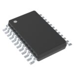 PI6C2410LE
The activity of extra discounts on wholesale prices is in full swing…
Please fill in your contact information and we will send you the latest wholesale price list.






